Underlayer film for copper, and a semiconductor device including the underlayer film
a technology of underlayer film and copper, which is applied in the direction of semiconductor/solid-state device details, coatings, chemical vapor deposition coatings, etc., can solve the problems of copper diffusion, lsi function is largely lost, and the resistivity is low, so as to prevent copper diffusion and improve the adhesion of copper film
- Summary
- Abstract
- Description
- Claims
- Application Information
AI Technical Summary
Benefits of technology
Problems solved by technology
Method used
Image

Examples
example 1
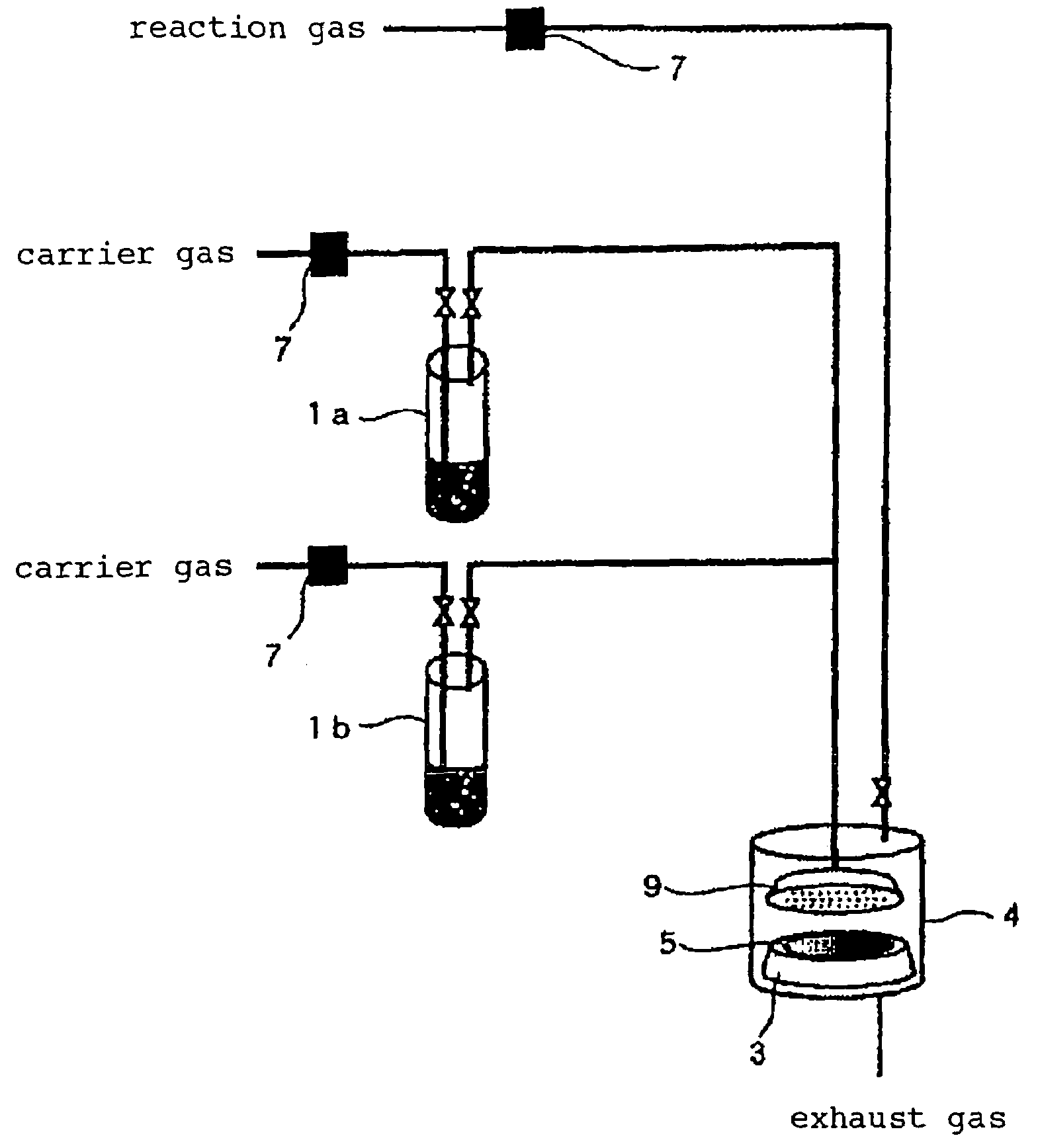
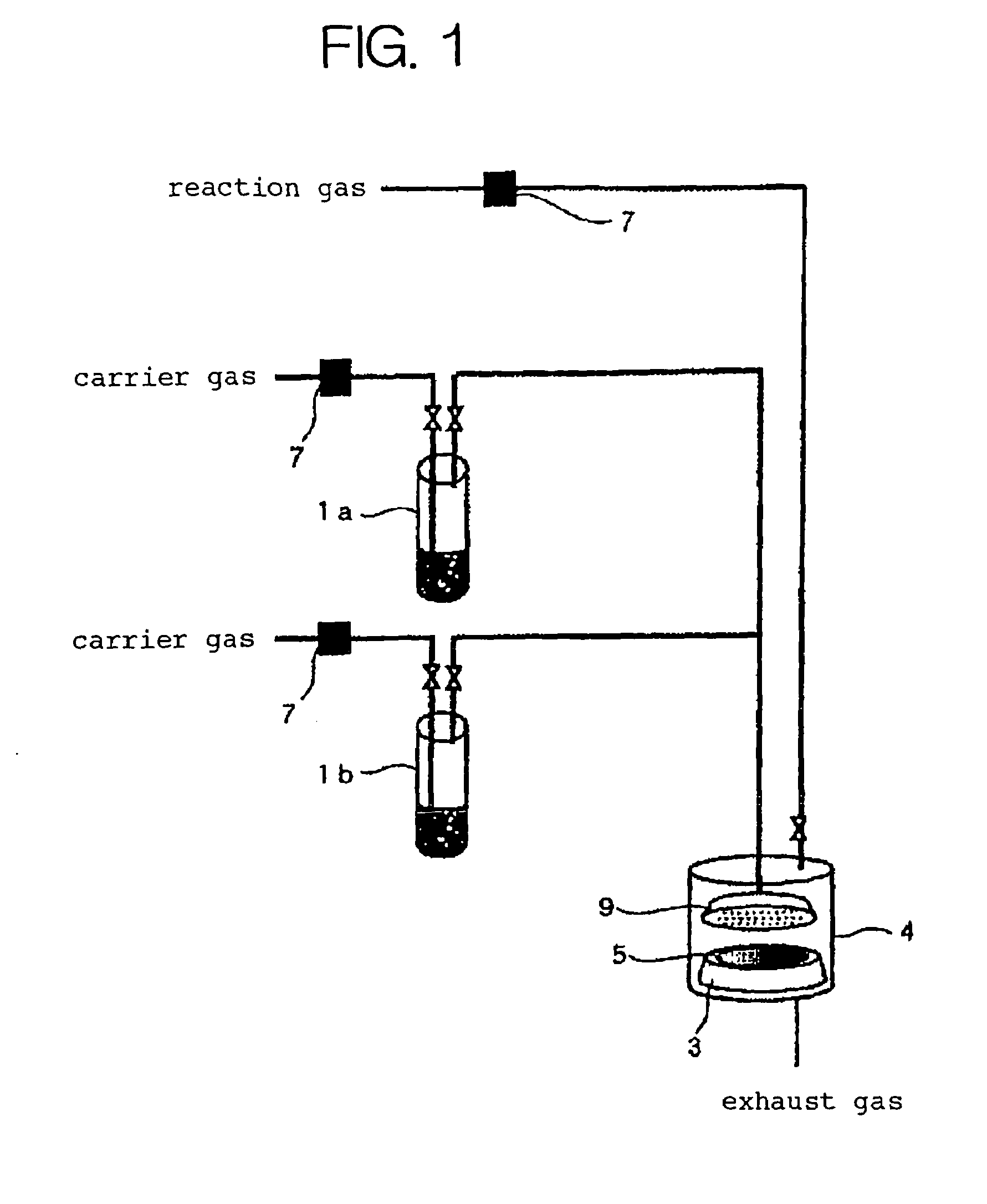
[0044]A silicon substrate with a SiO2 thermal oxide film formed on its surface was used as a substrate. The substrate, having its surface subjected to a Si—OH termination treatment, was immersed into a 1% by volume toluene solution of 1-diphenylphosphino-2-triethoxysilylethane heated to 60° C. for 1 hour. After 1 hour, the substrate was taken out of the solution, washed with toluene, and dried. Subsequently, the substrate was heated at 120° C. for 4 minutes to remove the residual solvent and byproduct.
[0045]The surface of the substrate obtained as above was measured using a reflectometer. The measurement showed that a nearly uniform thin film having a thickness of 1.2 nm was formed.
[0046]While measuring the thin film using FT-IR, peaks corresponding to Ph2PCH2CH2SiO— (where Ph represents a phenyl group) were observed.
[0047]After the formation of the thin film, a copper thin film having a thickness of 100 nm was formed by the CVD method using a hexafluoracetylacetonate copper trimeth...
examples 2 – 13
Examples 2–13
[0050]The procedure of Example 1 was repeated except that, instead of 1-dimethylphosphino-2-triethoxysilylethane used in Example 1,[0051]1-dimethylphosphino-2-triethoxysilylethane (Example 2),[0052]1-diethylphosphino-2-triethoxysilylethane (Example 3),[0053]1-dimethylphosphino-2-trimethoxysilylethane (Example 4),[0054]1-diethylphosphino-2-trimethoxysilylethane (Example 5),[0055]1-diphenylphosphino-2-trimethoxysilylethane (Example 6),[0056]1-dimethylphosphino-3-triethoxysilylpropane (Example 7),[0057]1-diethylphosphino-3-triethoxysilylpropane (Example 8),[0058]1-diphenylphosphino-3-triethoxysilylpropane (Example 9),[0059]1-diphenylphosphino-2-trichlorosilylethane (Example 10),[0060]1-diphenylphosphino-2-trisdimethylaminosilylethane (Example 11),[0061]1-diphenylphosphino-2-triisocyanatesilylethane (Example 12), and[0062]1-diphenylphosphino-4-triethoxysilylethylbenzene (Example 13) were used.
[0063]As a result, a thin film having a thickness of 1.2 to 2.2 nm in which a (R1R...
examples 14 – 26
Examples 14–26
[0064]Instead of the silicon substrate a SiO2 thermal oxidation film formed on its surface, a silicon substrate having an alkylsilicon-based film with a low dielectric constant was used in each of Examples 1 to 13, and was subjected to a similar process as above.
[0065]As a result, a thin film having a thickness of 1.2 to 2.2 nm in which a (R1R2)P—(R)n—Si group bonds to the substrate via a Si—O bond was formed in each of the examples. The adhesion of the copper thin film was examined for each example using the tape peeling test. In the test, peeling of the copper thin film was not observed in any of the examples. The copper diffusion to the underlayer film was also examined using the Back side SIMS for each example, but no copper diffusion was observed in any of the examples.
PUM
| Property | Measurement | Unit |
|---|---|---|
| Adhesion strength | aaaaa | aaaaa |
Abstract
Description
Claims
Application Information
 - R&D Engineer
- R&D Manager
- IP Professional
- Industry Leading Data Capabilities
- Powerful AI technology
- Patent DNA Extraction
Browse by: Latest US Patents, China's latest patents, Technical Efficacy Thesaurus, Application Domain, Technology Topic.
© 2024 PatSnap. All rights reserved.Legal|Privacy policy|Modern Slavery Act Transparency Statement|Sitemap