Array substrate and manufacturing method thereof

a technology of array substrate and manufacturing method, which is applied in the field of array substrate, can solve the problems of poor adhesion, deterioration of thin film transistor performance, and copper being hollowed out, and achieve the effect of improving the adhesion of the patterned metal member and blocking the diffusion of copper

Active Publication Date: 2021-12-30
TCL CHINA STAR OPTOELECTRONICS TECH LTD
View PDF0 Cites 0 Cited by
  • Summary
  • Abstract
  • Description
  • Claims
  • Application Information

AI Technical Summary

Benefits of technology

[0028]The present disclosure provides an array substrate and a manufacturing method thereof. A patterned metal member of the array substrate includes a patterned first metal layer, a patterned second metal layer, and a patterned copper layer which are sequentially disposed on a substrate. An etching rate at which an etching solution etches the second metal layer is less than another etching rate at which the etching solution etches the first metal layer. With the patterned second metal layer and the patterned first metal layer, a problem of metal residues in the second metal layer can be avoided, and a problem of copper hollowing caused by corrosion of the patterned second metal layer can be avoided. Moreover, an adhesion between the patterned first metal layer and the substrate is greater than an adhesion between the patterned copper layer and the substrate, which improves an adhesion of the patterned metal member on the substrate, and can block a diffusion of copper.

Problems solved by technology

However, the copper metal has poor adhesion to a glass and is prone to metal peeling Also, copper metal ions are prone to diffusion, which causes a performance of thin film transistors (TFTs) to deteriorate.
In a process using molybdenum metal as a bi-metal layer, because a copper / molybdenum structure is prone to bimetallic corrosion during a metal patterning process, and a copper metal corrosion will occur in a subsequent photoresist stripping process, resulting in the copper being hollowed out.
The hollowing out of copper can lead to a formation of metal tips.
In a subsequent manufacturing process, different layers of metals are prone to electrostatic breakdown, which greatly affects a product yield.
However, due to a presence of titanium metal in the molybdenum-titanium alloy, a wet etching solution containing fluorine must be used in a patterning process of the metal, which results in a low etching rate and is prone to a residue of molybdenum and titanium.

Method used


Image

  • Array substrate and manufacturing method thereof
  • Array substrate and manufacturing method thereof
  • Array substrate and manufacturing method thereof

Examples


Embodiment Construction

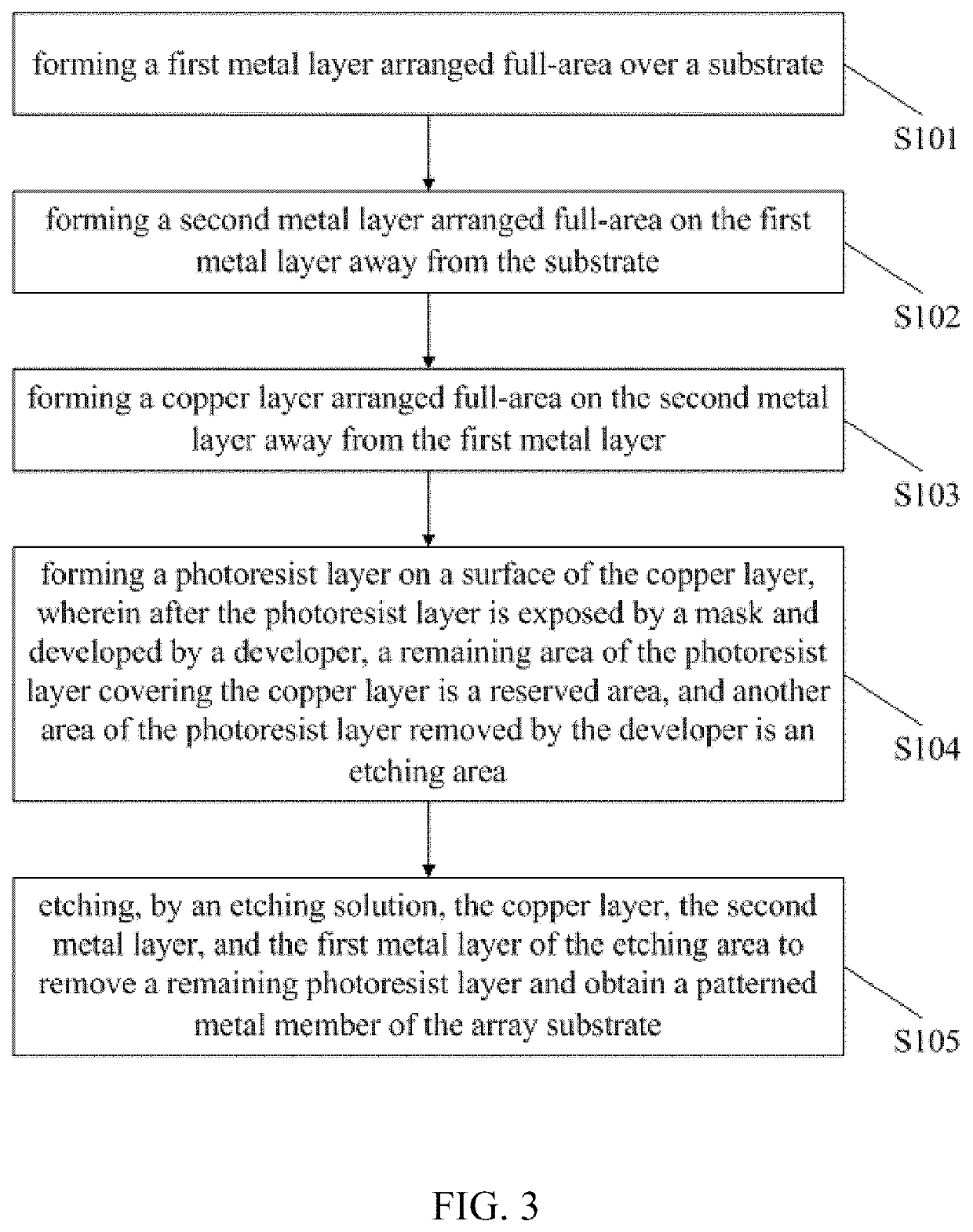
[0033]The technical solutions in the embodiments of the present disclosure are clearly and completely described herein with reference to the drawings in the embodiments of the present disclosure. Apparently, the described embodiments represent only some and not all of the embodiments of the present disclosure. All other embodiments obtained by one of ordinary skill in the art based on the embodiments of the present disclosure fall within the scope of protection of the present disclosure.

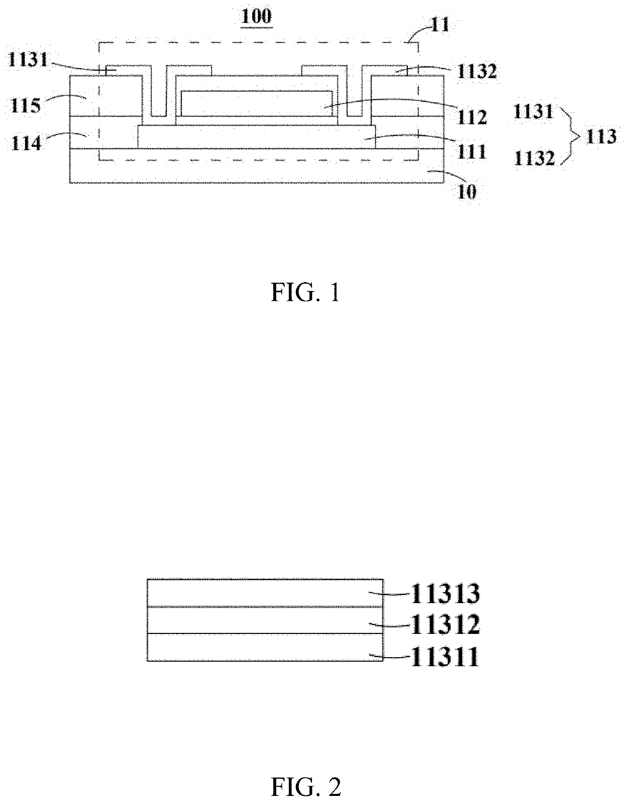
[0034]Please refer to FIG. 1 and FIG. 2. FIG. 1 is a schematic diagram of an array substrate of an embodiment of the present disclosure. FIG. 2 is a schematic diagram of a source / drain of the array substrate of FIG. 1. An array substrate 100 is a thin film transistor array substrate. The array substrate 100 can be used in a liquid crystal display panel or an organic light emitting diode display panel. The array substrate 100 includes a substrate 10, a plurality of thin film transistors 11, data lines...


PUM

PropertyMeasurementUnit
thicknessesaaaaaaaaaa
thicknessaaaaaaaaaa

Abstract

An array substrate and a manufacturing method thereof are provided. A patterned metal member of the array substrate includes a patterned first metal layer, a patterned second metal layer, and a patterned copper layer which are sequentially disposed on a substrate. An etching rate at which an etching solution etches the second metal layer is less than another etching rate at which the etching solution etches the first metal layer. An adhesion force between the patterned first metal layer and the substrate is greater than another adhesion force between the patterned copper layer and the substrate.

Description

FIELD OF DISCLOSURE[0001]The present disclosure relates to the field of display technologies, and in particular, to an array substrate and a manufacturing method thereof.BACKGROUND[0002]In high-generation liquid crystal display panels, metal wires made of copper materials have advantages of low impedance and strong resistance to electromigration, so they replace conventional metal wires made of aluminum materials. However, the copper metal has poor adhesion to a glass and is prone to metal peeling Also, copper metal ions are prone to diffusion, which causes a performance of thin film transistors (TFTs) to deteriorate. A metal layer is usually added to improve an adhesion between a copper metal layer and block the diffusion of copper. In a conventional manufacturing process of a display panel, the added metal layer is usually selected from molybdenum, titanium, and molybdenum-titanium alloy. In a process using molybdenum metal as a bi-metal layer, because a copper / molybdenum structur...

Claims


Application Information

Patent Timeline
Patent Type & Authority Applications(United States)
IPC IPC(8): H01L27/12
CPCH01L27/124H01L27/1222H01L27/127H01L27/1244H01L27/1259
Inventor CHEN, MENG
Owner TCL CHINA STAR OPTOELECTRONICS TECH LTD
Why Eureka
Try Eureka