Ground shield and related method

Inactive Publication Date: 2006-11-09
IBM CORP
View PDF10 Cites 9 Cited by
  • Summary
  • Abstract
  • Description
  • Claims
  • Application Information

AI Technical Summary

Benefits of technology

[0007] The invention includes a ground shield that includes a ‘cheesed’ metal positioned within a dielectric layer, and a metal region positioned within a first metal level over the cheesed metal. The ground shield can have different forms depending on the metal used, and provisions are made to prevent diffusion of copper (C

Problems solved by technology

As a result, the magnetic field dissipates power in the silicon, and degrades the quality factor of the RF passive element.
This approach, however, suffers from a number of drawbacks.
Accordingly, if the ground shield is made thicker, the aspect ratio of the metal wire is increased, which detrimentally results in higher

Method used


Image

  • Ground shield and related method
  • Ground shield and related method
  • Ground shield and related method

Examples


first embodiment

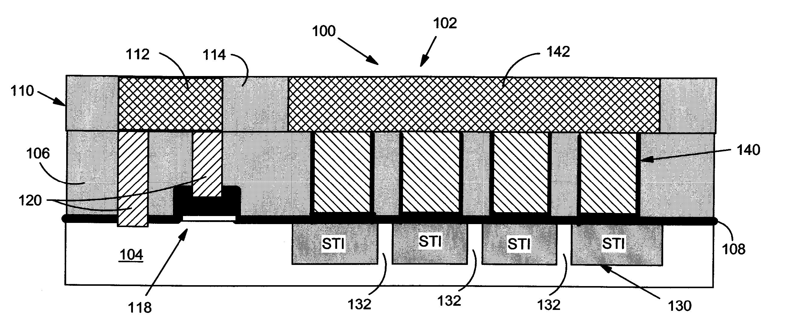
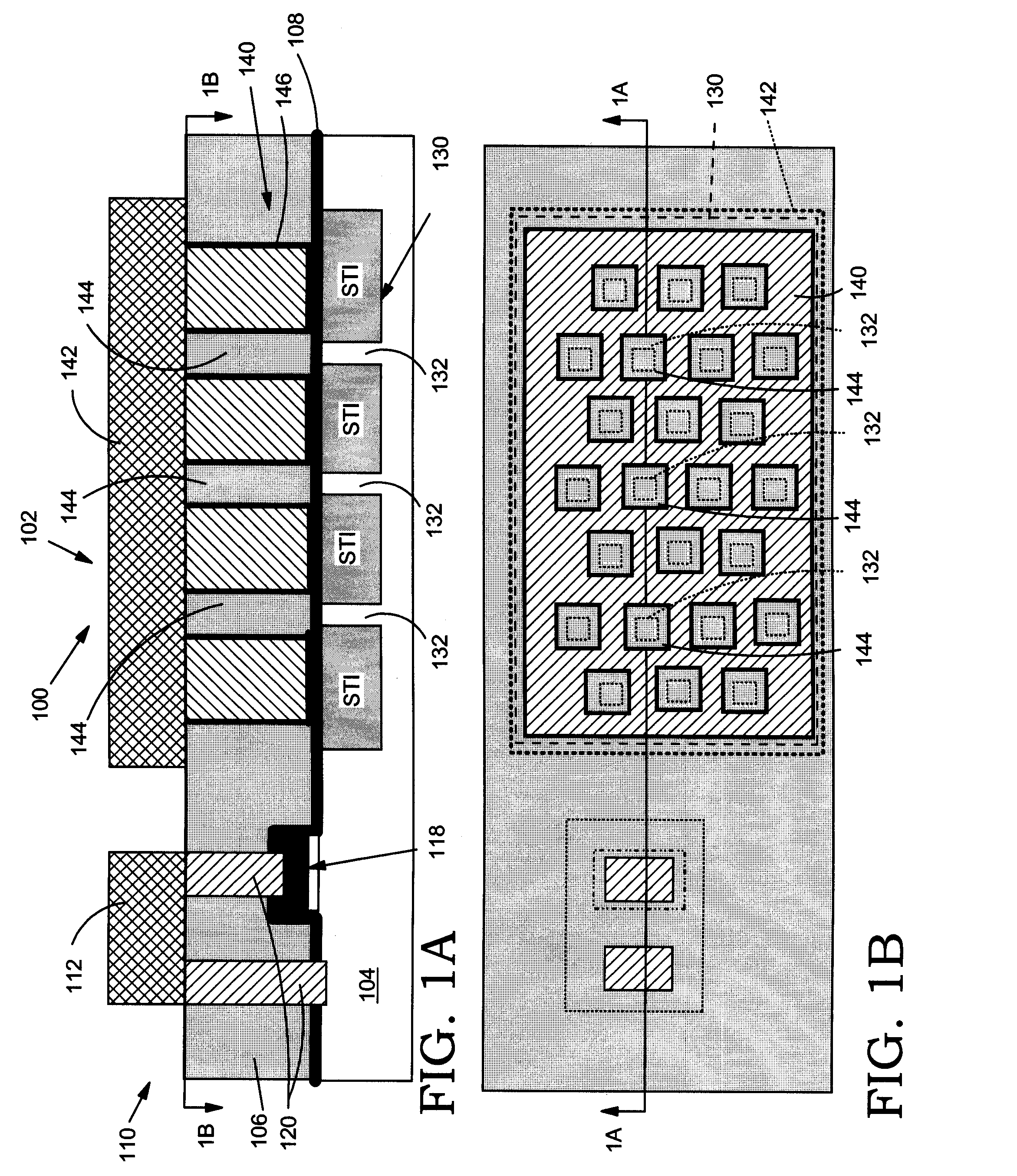
[0020] With reference to the accompanying drawings, FIGS. 1A-B show a ground shield 100 in accordance with the invention. FIG. 1B shows a plan view along line 1B-1B of FIG. 1A; similarly, FIG. 1A shows a cross-sectional view along line 1A-1A of FIG. 1B. Referring to the cross-sectional view of FIG. 1A, ground shield 100 includes a structure 102 including a substrate 104, i.e., of silicon, having a dielectric layer 106 positioned thereover. Dielectric layer 106 (hereinafter pre-metal dielectric (PMD) layer 106) may include any now known or later developed dielectric material, such as silicon dioxide (SiO2), hydrogenated silicon oxycarbide (SiCOH), phosphosilicate glass (PSG), boro-phosphosilicate glass (BPSG), etc., deposited using an known method such as plasma enhanced chemical vapor deposition (PECVD), high density plasma CVD (HDPCVD), sub-atmospheric CVD (SACVD), atmospheric pressure CVD (APCVD), atomic layer deposition (ALD), liquid phase chemical vapor deposition (LPCVD), or th...

second embodiment

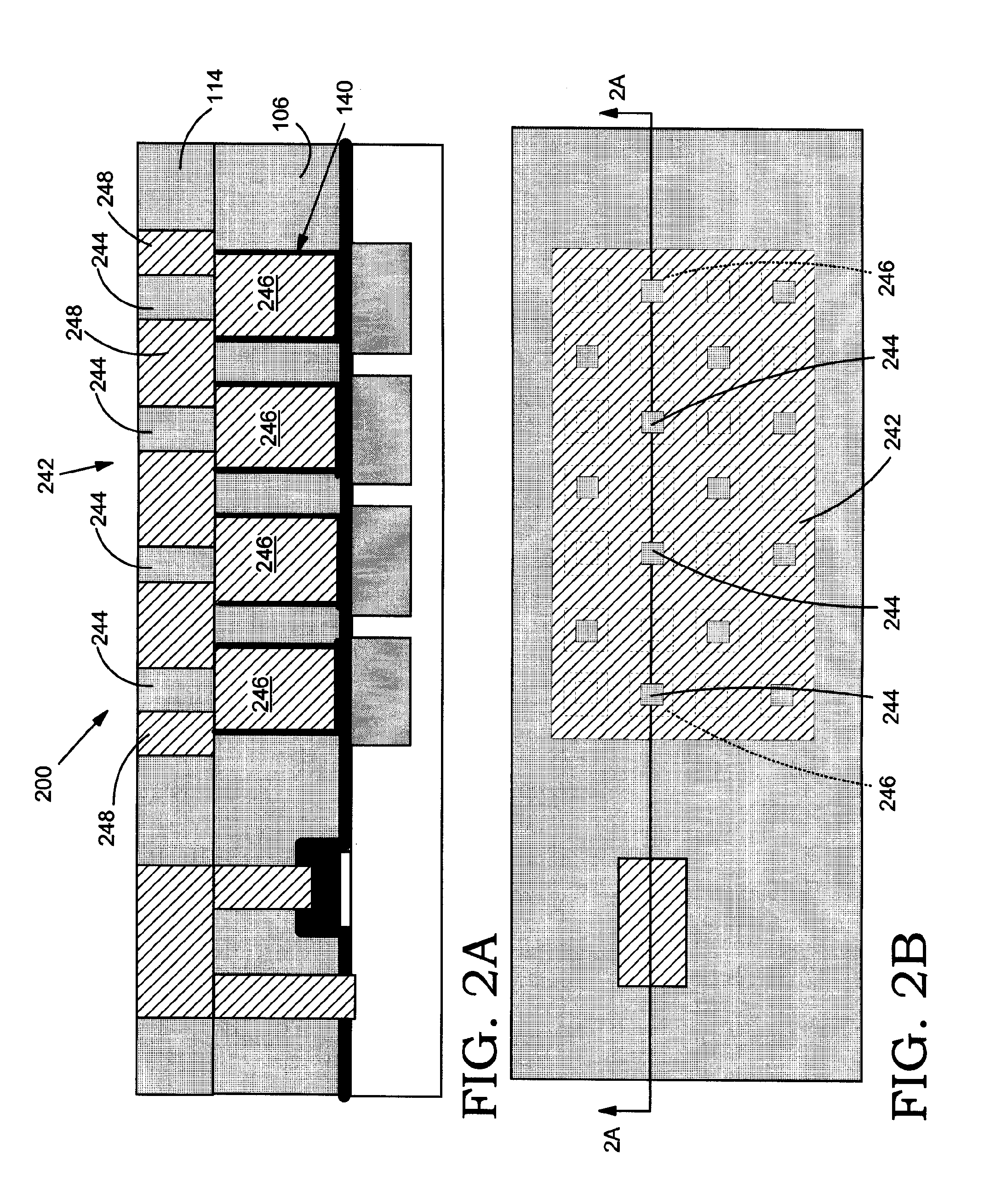
[0025] FIGS. 2A-B show a ground shield 200. FIG. 2B shows a plan view of FIG. 2A, and FIG. 2A shows a cross-sectional view along line 2A-2A of FIG. 2B. Ground shield 200 is substantially similar to ground shield 100 of FIGS. 1A-B, except that it includes a cheesed metal region 242 to prevent dishing because region 242 is fabricated using a damascene process unlike layer 110 (FIG. 1A), which is fabricated using a subtractive etch process. Cheesed metal region 242 is positioned in an inter-metal dielectric (IMD) layer 114. IMD layer 114 may include any now known or later developed inter-metal dielectric material. Typical inter-metal dielectric layers are deposited using spin-on, or PECVD methods and can include SiO2, fluorinated SiO2, SiCOH, porous SiCOH, silicon low-k dielectric (SiLK™) (available from Dow Chemical), and the like. That is, in certain instances, metal region 142 (FIGS. 1A-B) may be so large that it requires cheesing to prevent dishing during chemical mechanical polish...


PUM


Abstract

A ground shield is disclosed that includes a ‘cheesed’ metal positioned within a dielectric layer and a metal region positioned within a first metal level over the cheesed metal. The ground shield can have different forms depending on the metal used, and provisions are made to prevent diffusion of copper (Cu) when that is used as the metal in the cheese metal of the ground shield. The ground shield provides a low resistance, very thick metal at a first metal (M1) level for passive RF elements in conjunction with the standard back-end-of-line (BEOL) integration. The invention also includes a method of forming the ground shield.

Description

BACKGROUND OF THE INVENTION [0001] 1. Technical Field [0002] The present invention relates generally to semiconductor fabrication, and more particularly, to a ground shield for a semiconductor device and a related method. [0003] 2. Related Art [0004] In silicon radio frequency (RF) applications, magnetic fields created by current flowing through RF passive elements (e.g., inductors, capacitors, transmission lines, etc.) creates eddy currents in the underlying conductors and silicon substrate. As a result, the magnetic field dissipates power in the silicon, and degrades the quality factor of the RF passive element. To address this situation, the lossy silicon substrates are often shielded from RF passive elements by a metal ground shield or ground plane, which provides a low resistance return path for the magnetic field-induced electrical current. A ground shield is typically located on top of the silicon substrate and under the RF passive element to block eddy currents from entering...

Claims


Application Information

Patent Timeline
IPC IPC(8): H01L23/52
CPCH01L23/5225H01L2924/0002H01L2924/00
Inventor ERTURK, METEJOSEPH, ALVIN J.STAMPER, ANTHONY K.
Owner IBM CORP
Why Eureka
Try Eureka