Semiconductor device

a technology of semiconductor devices and semiconductors, applied in semiconductor devices, basic electric elements, instruments, etc., can solve problems such as increase in layout area, and achieve the effects of reducing the layout area, preventing copper diffusion, and reducing the line width of fuses

Active Publication Date: 2011-05-19
RENESAS ELECTRONICS CORP
View PDF9 Cites 23 Cited by
  • Summary
  • Abstract
  • Description
  • Claims
  • Application Information

AI Technical Summary

Benefits of technology

[0009]The present invention has been made in view of the above circumstances and has an object to provide a semiconductor device capable of reducing the line width of a fuse.
[0010]Another object of the present invention is to provide a semiconductor device capable of reducing the layout area.
[0011]A semiconductor device according to the present invention is a semiconductor device having a plurality of metal wiring layers, the semiconductor device comprising: a fuse which is formed using a first copper wire in a metal wiring layer upper than the lowermost metal wiring layer of the metal wiring layers and which stores a data signal by being melted or not; a dummy fuse provided adjacent to the fuse and formed using a second copper wire in the same metal wiring layer as that of the fuse; and a diffusion protective wall which is formed using the metal wiring layers so as to surround the fuse and the dummy fuse and which prevents diffusion of copper. Here, each wiring width of the fuse and the dummy fuse is set to the minimum line width in a region surrounded by the diffusion protective wall, and wherein the interval between the fuse and the dummy fuse is set to the minimum interval in the region surrounded by the diffusion protective wall.
[0012]Another semiconductor device according to the present invention is a semiconductor having a plurality of metal wiring layers, the semiconductor device comprising a memory array including: a plurality of fuses arranged in a plurality of rows and columns and each of which stores a data signal by being melt or not; a plurality of word lines provided corresponding to the rows, respectively; a plurality of bit lines provided corresponding to the columns, respectively; and a plurality of transistors each provided corresponding to each of the fuses and each of which has a gate coupled to the corresponding word line. Each of the fuses and the transistor corresponding thereto are coupled in series between a fuse power source node and the corresponding bit line. Each of the fuses is formed using a first copper wire in a metal wiring layer upper than the lowermost metal wiring layer of the metal wiring layers. The semiconductor device further includes: a row decoder that sets any of the word lines to a selection level according to a row address signal and turns on the transistor corresponding to the word line; a column decoder that selects any of the bit lines according to a column address signal; a write circuit that melts the selected fuse by applying a predetermined voltage between the fuse power source node and the bit line selected by the column decoder at the time of write operation; a read circuit that detects whether or not an electric current flows between the fuse power source node and the bit line selected by the column decoder and outputs a data signal at a logic level in accordance with the detection result at the time of read operation; and a diffusion protective wall formed using a metal wire in the same metal wiring layer as that of the fuses so as to surround at least the fuses and which prevents diffusion of copper.
[0013]In a semiconductor device according to the present invention, the dummy fuse is provided adjacent to the fuse, each wiring width of the fuse and the dummy fuse is set to the minimum line width, and the interval between the fuse and the dummy fuse is set to the minimum interval. Consequently, the exposure condition of the fuse and the dummy fuse is optimized, and therefore, it is possible to form a fuse with a minimum line width.
[0014]Further, in another semiconductor device according to the present invention, the fuses are surrounded by one diffusion protective wall, and therefore, it is possible to reduce the layout area compared to the conventional case where each fuse is surrounded by the diffusion protective wall.

Problems solved by technology

However, in the manufacturing process of a 100 nm or less node, there is such a problem that even if a fuse, which is an isolated copper wire, is designed to have a minimum line width, in fact, the fuse is formed thicker than the minimum line width.
In Patent Document 1, there is such a problem that when the number of fuses increases, the layout area increases because the diffusion protective wall is provided for each fuse.

Method used


Image

  • Semiconductor device
  • Semiconductor device
  • Semiconductor device

Examples


first embodiment

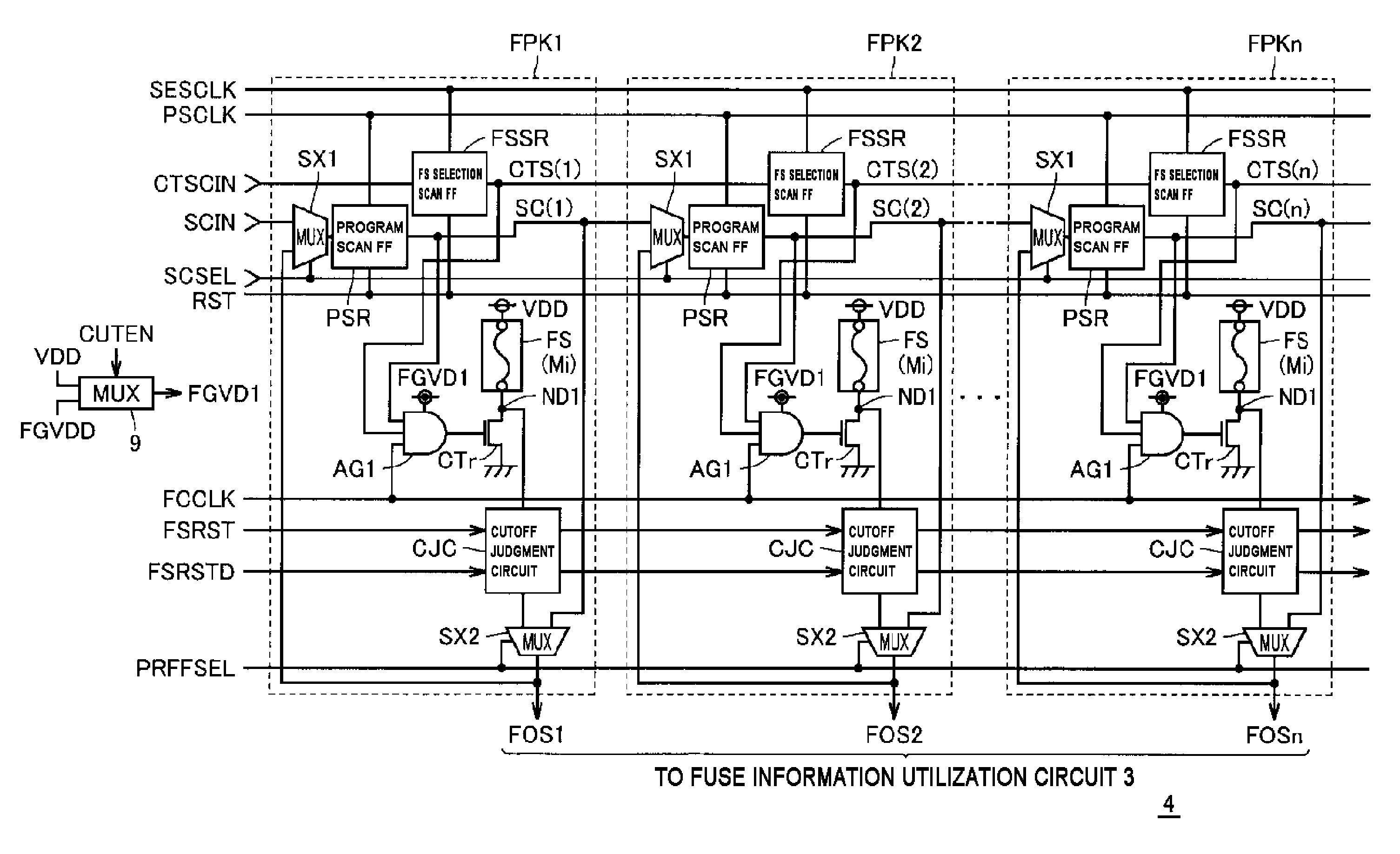
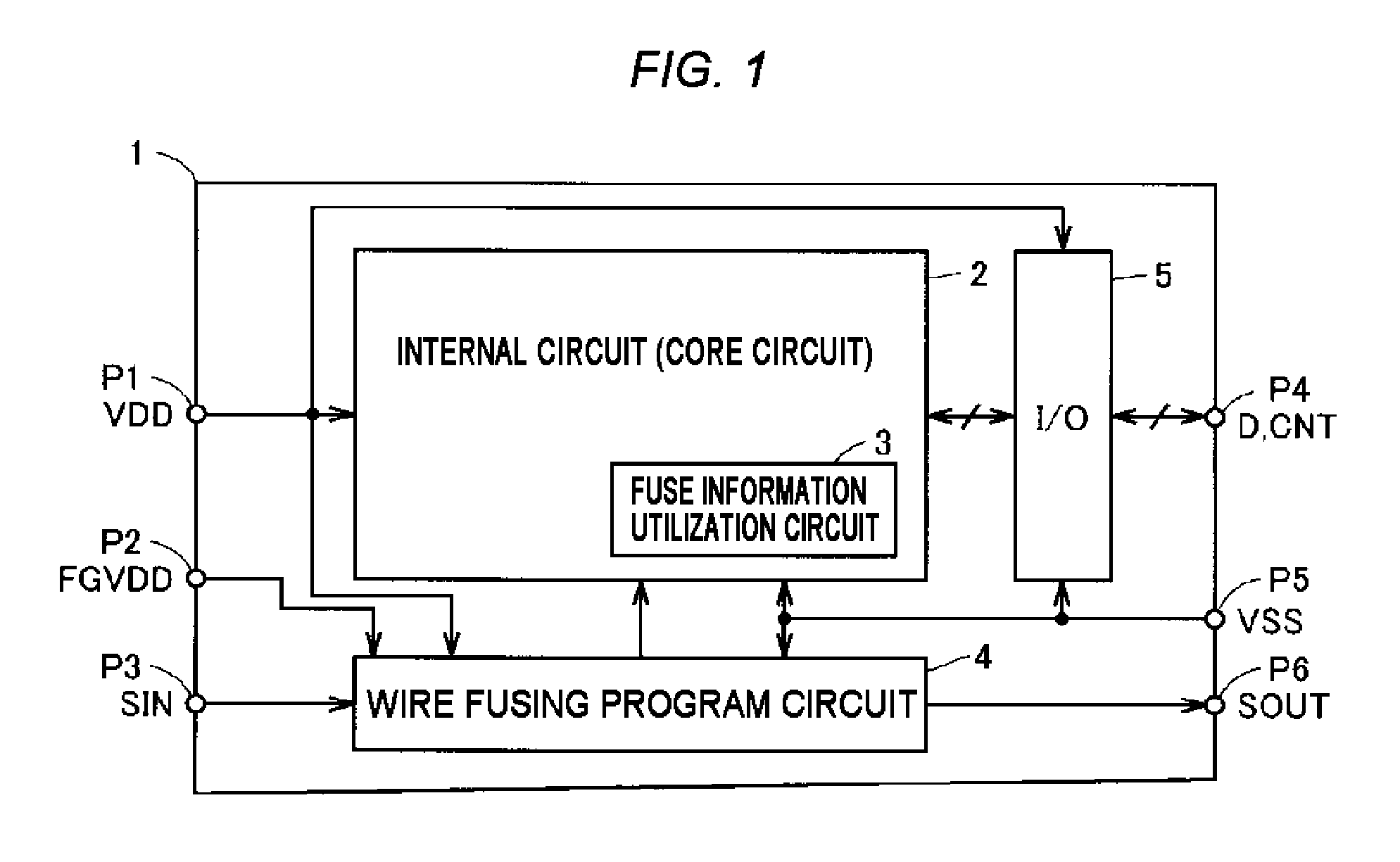
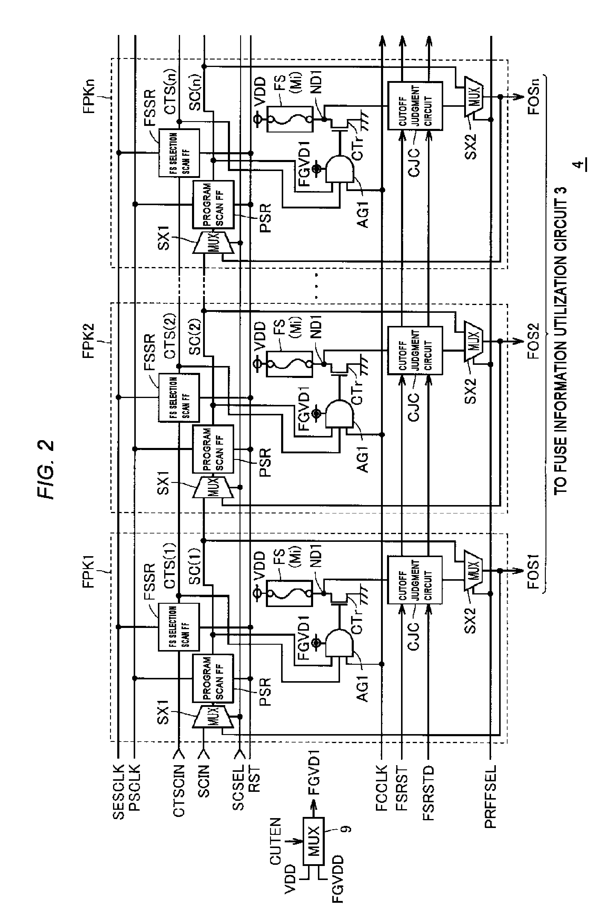
[0056]FIG. 1 is a diagram roughly showing a general configuration of a semiconductor device according to a first embodiment of the present invention. In FIG. 1, a semiconductor device 1 includes an internal circuit (core circuit) 2 that realizes predetermined functions, a wire fusing program circuit 4 that fixedly stores information that specifies the operation state or operation aspect of the internal circuit 2 (information on the internal circuit), and a signal input / output (I / O) circuit 5.

[0057]The semiconductor device 1 may be formed over one semiconductor chip or integrated over the same chip as that of the functional blocks, such as another processor and a memory, and the semiconductor device is equivalent to a semiconductor integrated circuit device.

[0058]The internal circuit 2 receives a ground voltage VSS given from outside via a ground pad P5 as a reference voltage as well as receiving a power source voltage VDD given from outside via a power source pad P1 as an operating ...

first modified example

[0178]FIG. 26 is a diagram showing a first modified example of the first embodiment, to be compared with FIG. 10. In FIG. 26, in the first modified example, a plurality (eight in the figure) of the dummy fuses DFU is arranged on both sides of the fuse FU, respectively. The fuse FU extends in the longitudinal direction and the dummy fuses DFU extend in the transverse direction.

[0179]Each wiring width of the fuse FU and the dummy fuse DFU is set to the minimum line width in the fuse formation region. The interval between the fuse FU and each dummy fuse DFU is set to the minimum interval in the fuse formation region. The dummy fuses DFU are arranged at equal intervals and the interval between the two neighboring dummy fuses DFU is set to the minimum interval in the fuse formation region. Therefore, since the exposure condition of the fuse FU and the dummy fuse DFU is optimized by the OPC in the manufacturing process, it is possible to form the fuse FU with the minimum line width.

[0180]...

second modified example

[0181]FIG. 28 is a section view showing a second modified example of the first embodiment, to be compared with FIG. 5. In FIG. 28, on the surface of a P-type well (P well) 130, N-type active regions (impurity regions) 134a to 134d are formed spaced from one another. Under the P well 130, a deep N well 132 is formed and thereby the P well 130 is separated from other circuit formation regions. The P well 130 is disposed commonly in the fuse program circuit.

[0182]Over the surface of the P well 130 between the impurity regions 134a to 134d, gate electrode wires 136a, 136b, and 136c formed by, for example, polysilicon, are arranged. These gate electrode wires 136a to 136c and the active regions (impurity regions) 134a to 134d form the fusing current supply transistor CTr. That is, the fusing current supply transistor CTr is configured by a plurality of unit MOS transistors arranged in parallel and these unit MOS transistors are formed by the active regions and the gate electrode wires sh...


PUM


Abstract

To provide a semiconductor device capable of reducing the line width of a fuse.
In the semiconductor device, a dummy fuse is provided adjacent to a fuse, each wiring width of the fuse and the dummy fuse is set to the minimum line width, and the interval between the fuse and the dummy fuse is set to the minimum interval. Consequently, the exposure condition of the fuse and the dummy fuse is optimized by OPC, and therefore, it is possible to form the fuse with the minimum line width.

Description

CROSS-REFERENCE TO RELATED APPLICATION[0001]The disclosure of Japanese Patent Application No. 2009-260911 filed on Nov. 16, 2009 including the specification, drawings and abstract is incorporated herein by reference in its entirety.BACKGROUND OF THE INVENTION[0002]The present invention relates to a semiconductor device and particularly, to a semiconductor device that comprises a fuse for storing a data signal by being melted or not.[0003]In a semiconductor integrated circuit device (semiconductor device), a fuse program circuit is used for various applications. In the fuse program circuit, the state of an output signal is set fixedly depending on whether a fuse element is melted or not. For example, in order to fine-adjust (trim) the constant of an analog circuit, such a fuse element is used. Specifically, programming (melt / not melt) of a fuse element is performed for the adjustment of the current drive force of a transistor element, the adjustment of the amount of supply current of...

Claims


Application Information

Patent Timeline
Patent Type & Authority Applications(United States)
IPC IPC(8): G11C17/16H01L23/525G11C17/18
CPCG11C17/18G11C17/16
Inventor OBAYASHI, SHIGEKI
Owner RENESAS ELECTRONICS CORP
Why Eureka
Try Eureka