Semiconductor device

a technology of semiconductor devices and semiconductors, applied in semiconductor devices, semiconductor/solid-state device details, instruments, etc., can solve the problems of leak current flow, increase the number of wiring layers necessary for a fuse element, and increase the cost of wiring resources. , to achieve the effect of preventing the diffusion of copper atoms at the time of cutting a fuse, reducing the number of wiring layers necessary for a fuse element, and reducing the occupation area of the fuse elemen

Active Publication Date: 2010-09-16
RENESAS ELECTRONICS CORP
View PDF2 Cites 39 Cited by
  • Summary
  • Abstract
  • Description
  • Claims
  • Application Information

AI Technical Summary

Benefits of technology

[0015]By using the power supply wire as a prevention cover wire just above the fuse, the number of wiring layers necessary for a fuse element can be reduced, and the occupation area of the fuse element can be also reduced.
[0016]By setting the second power supply voltage to the ground voltage in the normal operation mode, diffusion of copper atoms at the time of cutting a fuse can be prevented, and occurrence of adverse influence on a periphery circuit can be prevented.

Problems solved by technology

Consequently, a problem occurs that wiring resources are consumed more than necessary, and there is still room for improvement in reduction in the wiring resources.
Consequently, there is the possibility that when a fuse is in a not-cut state, leak current flows in a transistor for supplying fusing current.
A complicated circuit control configuration for suppressing the leak current is required.
Consequently, the cover is wide and there is a problem such that, at the time of manufacturing a cover is excessively dent by dishing of CMP (Chemical Mechanical Polishing).

Method used


Image

  • Semiconductor device
  • Semiconductor device
  • Semiconductor device

Examples


first embodiment

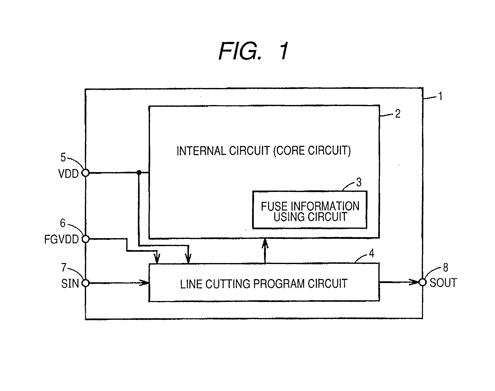
[0081]FIG. 1 is a diagram schematically showing the configuration of an entire semiconductor device according to a first embodiment of the present invention. In FIG. 1, a semiconductor device 1 includes an internal circuit (core circuit) 2 realizing a predetermined function and a line cutting program circuit 4 that fixedly storing information specifying an operation state or an operation mode of the internal circuit 2 (information related to the internal circuit).

[0082]The semiconductor device 1 may be formed on a single semiconductor chip or may be integrated on a chip together with a function block of another processor, memory, or the like. The semiconductor device is equivalent to a semiconductor integrated circuit device.

[0083]The internal circuit 2 receives a power supply voltage VDD applied from the outside via a power supply node (pad) 5 as an operation power voltage and realizes the predetermined function. The internal circuit 2 is a core circuit of the semiconductor device ...

second embodiment

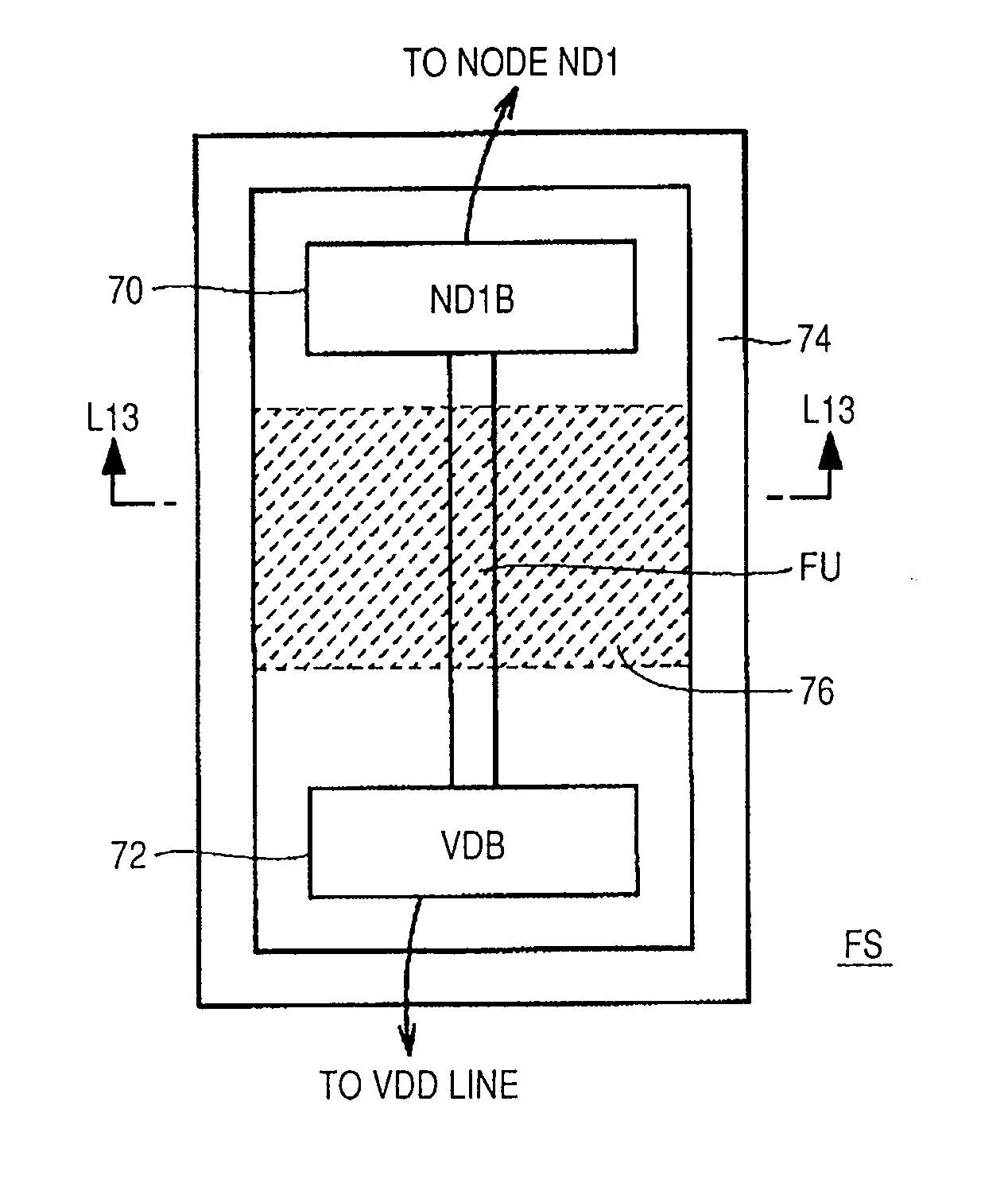
[0195]FIG. 12 is a diagram schematically showing the configuration of the fuse element FS according to a second embodiment of the present invention. In FIG. 12, the fuse element FS includes the fuse FU. The fuse FU is formed by a copper (Cu) wire and is realized by using the metal wire in an upper layer above a third metal wire layer. In the second embodiment, the fuse element FU is formed by using the wire in a fourth metal wire layer.

[0196]The fuse FU is coupled to a not-shown power supply line via a wide wire bed region VDB and is coupled to a wire region realizing the node ND1 via a node bed region ND1B. A copper diffusion preventing wall structure 74 is disposed so as to surround the fuse FU and the bed regions VDB and ND1B. The configuration of the copper diffusion preventing wall structure 74 will be described in detail later. An upper-part diffusion preventing wall wire 76 formed so as to cover at least a cut part in the fuse FU is included in an upper layer of the fuse FU. ...

third embodiment

[0270]FIG. 26 is a diagram schematically showing a sectional structure of a fuse element according to a third embodiment of the invention. In FIG. 26, a deep N well 202 is provided below a P well 200. The P well 200 and the deep N well 202 are disposed commonly to a fuse element in a fuse box. The fuse box refers to a region in which a plurality of fuse elements are aligned.

[0271]In the surface of the P well 200, active regions (N-type impurity regions) 204a to 204d are disposed at intervals. Active regions 204x and 204y are disposed in adjacent fuse element regions. The impurity regions 204 and 204d are shared by fusing current supply transistors for the fuse elements included in the adjacent fuse program circuits.

[0272]In the surface of the P well 200, gate electrode wires 206a, 206b, and 206c are disposed via a gate insulating film between the impurity regions 204a and 204b, between the impurity regions 204b and 204c, and between the impurity regions 204c and 204d. Also in the ad...


PUM


Abstract

The present invention provides a semiconductor device realizing reliable cutting of a fuse without enlarging layout area of a fuse element and the reduced number of wiring layers of a preventing wall that prevents diffusion of fuse copper atoms. A fuse is formed by using a wire in a metal wiring layer as an upper layer in a plurality of metal wiring layers. Wires are disposed just above and just below a fuse each with a gap of at least two wiring layers. In an upper layer, a power wire that transmits power supply voltage is used as a part covering a preventing wall structure just above the fuse.

Description

CROSS-REFERENCE TO RELATED APPLICATIONS[0001]The disclosure of Japanese Patent Application No. 2009-56761 filed on Mar. 10, 2009 including the specification, drawings and abstract is incorporated herein by reference in its entirety.BACKGROUND OF THE INVENTION[0002]The present invention relates to a semiconductor device and, particularly, to a semiconductor device having a fuse program circuit including a fuse element that stores fixed information. More specifically, the invention relates to a configuration for realizing a fuse program circuit capable of reliably cutting a fuse element with low power consumption and smaller occupation area and performing a cut state determination.[0003]In a semiconductor integrated circuit device (semiconductor device), a fuse program circuit is used for various applications. A state of an output signal of the fuse program circuit is fixedly set according to whether a fuse element is cut or not. For example, to finely adjust the constant of an analog...

Claims


Application Information

Patent Timeline
Patent Type & Authority Applications(United States)
IPC IPC(8): H01L23/525
CPCG11C17/18H01L23/5256H01L2924/3011H01L2924/0002H01L2924/00
Inventor OBAYASHI, SHIGEKI
Owner RENESAS ELECTRONICS CORP
Why Eureka
Try Eureka