Memory array having a layer with electrical conductivity anisotropy

a memory array and anisotropy technology, applied in the field of electric hysteretic technology memories, can solve the problems of low areal bit density limit on feram data storage, complex mask structure, and high cost, and achieve the effect of increasing electrical conductivity

Inactive Publication Date: 2006-04-11
SEAGATE TECH LLC
View PDF9 Cites 23 Cited by
  • Summary
  • Abstract
  • Description
  • Claims
  • Application Information

AI Technical Summary

Benefits of technology

[0008]Other features and benefits that characterize embodiments of the present invention will be apparent upon reading the following detailed description and review of the associated drawings.

Problems solved by technology

The masked structures are complex and expensive, and the resolution limits of the masking technology sets an undesirable low areal bit density limit on FeRAM data storage.

Method used


Image

  • Memory array having a layer with electrical conductivity anisotropy
  • Memory array having a layer with electrical conductivity anisotropy
  • Memory array having a layer with electrical conductivity anisotropy

Examples


Embodiment Construction

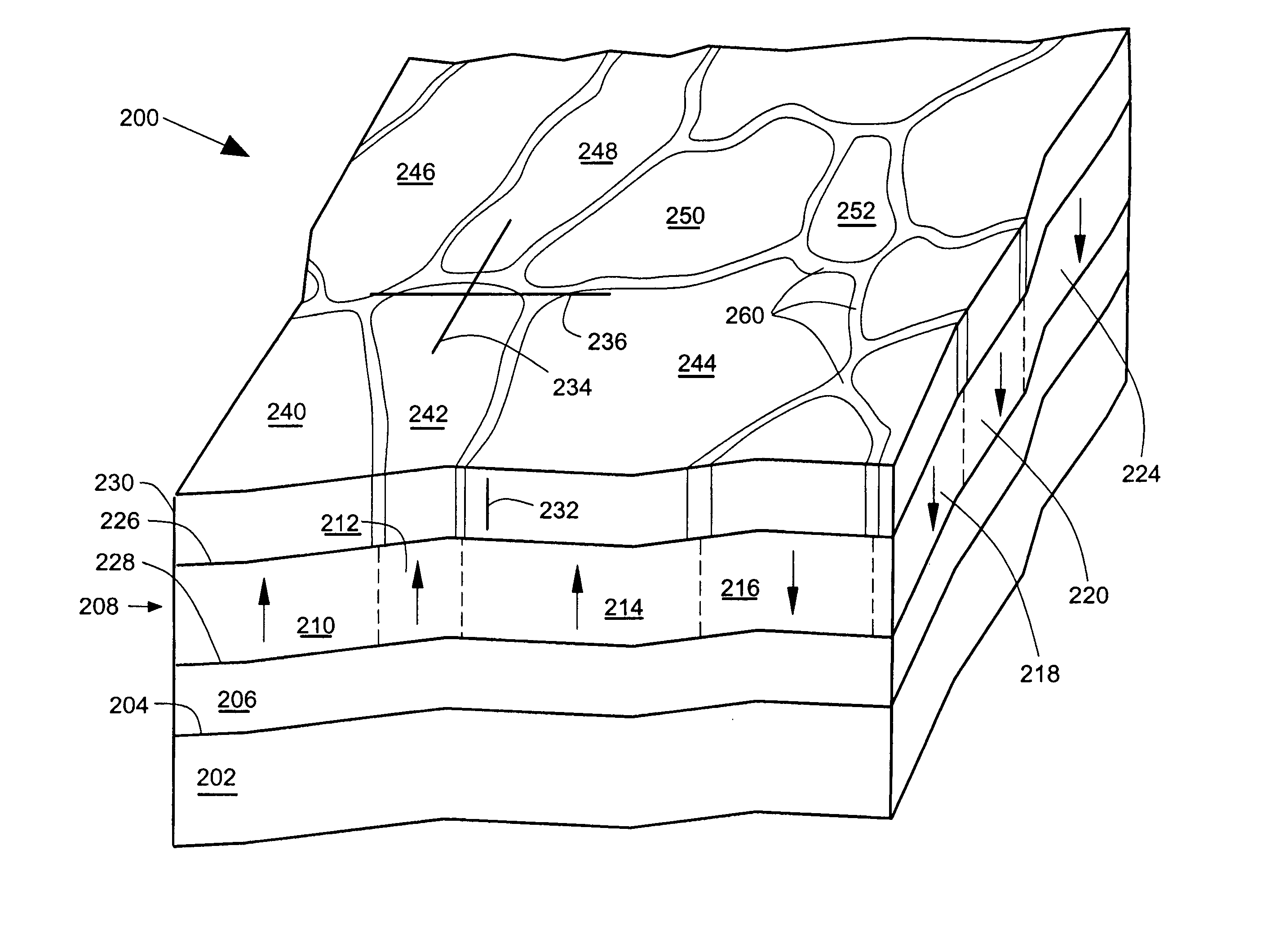
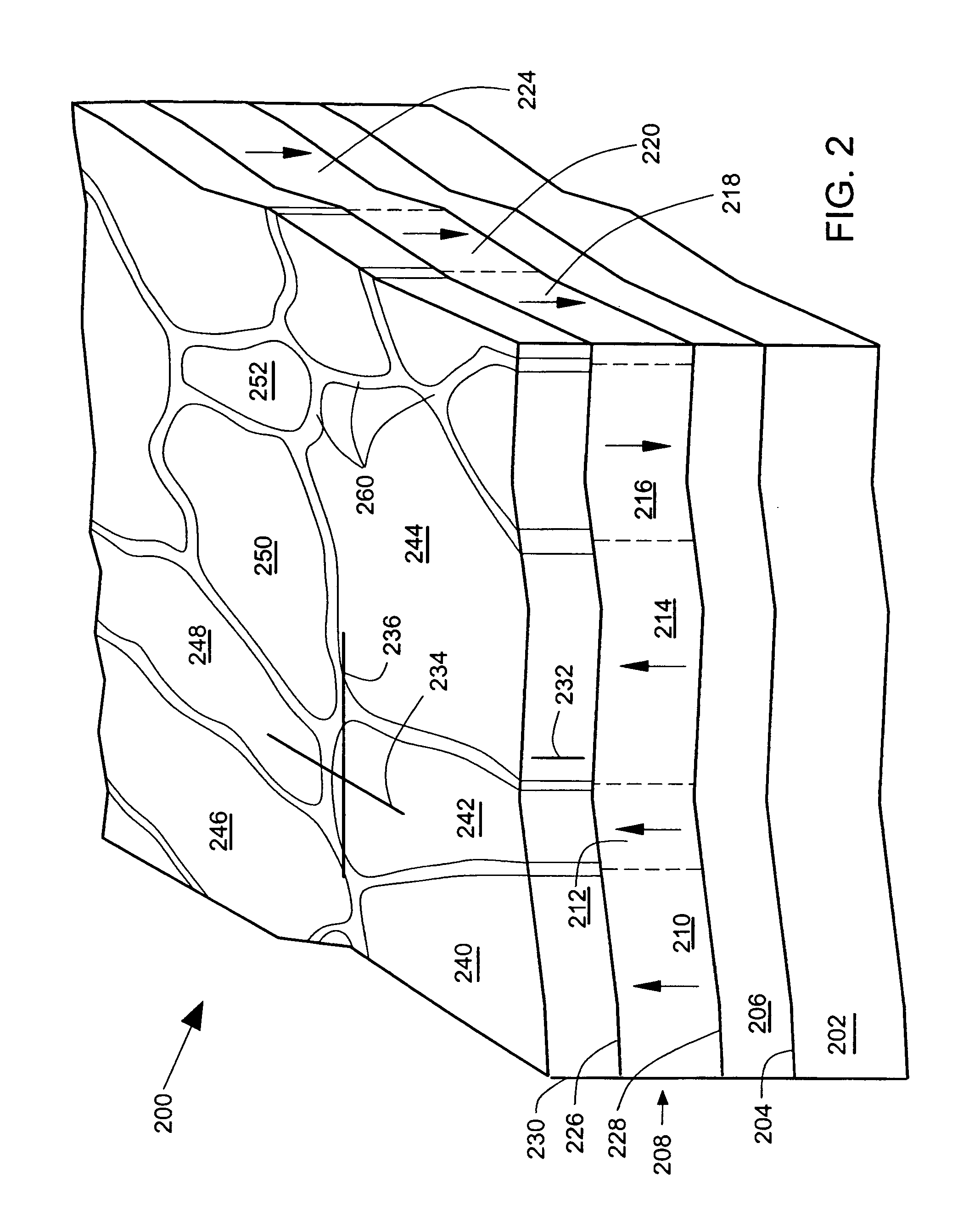
[0017]In the embodiments described below, a memory array includes a memory layer of hysteretic material that is covered with a conductive layer that is electrically anisotropic. The conductive layer includes higher conductivity islets that are separated from one another by a lower conductivity matrix. The islets are formed and defined inherently by the molecular characteristics of a deposition process used for the conductive layer. There is no need to provide any masking steps in order to define either the islets or individual memory domains. The individual memory domains are defined by an area swept by a trailing edge of a moving contact probe during a write pulse. Individual islets of hysteretic material can be written to and read electrically. The hysteretic material can comprise electrically polarizable material such as PZT film. Alternatively, the hysteretic material can comprise a phase change material, such as a chalcogenic material, that can change phase from crystalline to ...


PUM

PropertyMeasurementUnit
diameteraaaaaaaaaa
mean diameteraaaaaaaaaa
diameteraaaaaaaaaa

Abstract

A memory array includes a memory layer that has hysteretic domains with domain axes extending between first and second memory layer surfaces. A conductive layer on the first memory layer surface has anisotropically increased electrical conductivity in a thickness direction. A movable conductive probe has a contact area on the conductive layer and moves to access a selected hysteretic domain.

Description

FIELD OF THE INVENTION[0001]The present invention relates generally to electrical hysteretic technology memories, and more particularly, but not by limitation, to electrically hysteretic memories such as ferroelectric random access memories (FeRAM) and phase change memories.BACKGROUND OF THE INVENTION[0002]Ferroelectric random access memories (FeRAM) are typically arranged in rectangular arrays of ferroelectric cells with multilayered masked structures that delineate the cells, and row and column metallizations separated by insulating layers for addressing individual cells. The masked structures typically also include masked structures defining transistors for controlling current flow to individual cells.[0003]The masked structures are complex and expensive, and the resolution limits of the masking technology sets an undesirable low areal bit density limit on FeRAM data storage. There is a need to provide electrical hysteresis methods and devices that are not limited by use of maski...

Claims


Application Information

Patent Timeline
Patent Type & Authority Patents(United States)
IPC IPC(8): H01L29/76G11B9/02G11B9/04
CPCG11B9/04G11B9/02
Inventor AHNER, JOACHIM WALTERYU, JUNWELLER, DIETER KLAUS
Owner SEAGATE TECH LLC
Why Eureka
Try Eureka