Circuit verification

a technology of circuit verification and verification process, applied in the field of circuit verification, can solve the problems of affecting the operation of the system, and requiring more advanced and complex verification process and procedures, so as to reduce or eliminate the disadvantages and problems

Inactive Publication Date: 2006-04-11
FUJITSU LTD
View PDF6 Cites 13 Cited by
  • Summary
  • Abstract
  • Description
  • Claims
  • Application Information

AI Technical Summary

Benefits of technology

[0005]Particular embodiments of the present invention may reduce or eliminate disadvantages and problems traditionally associated with circuit verification.
[0007]Particular embodiments of the present invention may provide one or more technical advantages. Particular embodiments increase efficiency of partitioned ordered binary decision diagram (POBDD)-based verification of circuits. Particular embodiments reduce time requirements associated with POBDD-based verification of circuits. Particular embodiments reduce memory requirements associated with POBDD-based verification of circuits. Particular embodiments reduce memory costs associated with POBDD-based verification of circuits. Particular embodiments provide superlinear speedup in the event of one or more circuit errors. Particular embodiments reduce the occurrence of space blowup in POBDD-based verification of circuits.
[0008]Particular embodiments provide a systematic method for covering a state space. Particular embodiments increase time and space efficiency of semiformal verification. Particular embodiments provide improved distribution of state-space coverage, such that state-space coverage is less localized. In particular embodiments, a continuous spectrum of time, memory, and coverage tradeoff is possible. In particular embodiments, less useful partitions are ignored according to a scheduling technique. In particular embodiments, only relatively easy states are covered, but uniform distribution is at least attempted.

Problems solved by technology

These rigorous demands associated with production and design generally result in the need for more advanced and complex verification processes and procedures.
Flaws or inaccuracies in an IC or a digital element may inhibit system functionality and / or cause significant operational problems in a corresponding architecture.

Method used


Image

  • Circuit verification
  • Circuit verification
  • Circuit verification

Examples


Embodiment Construction

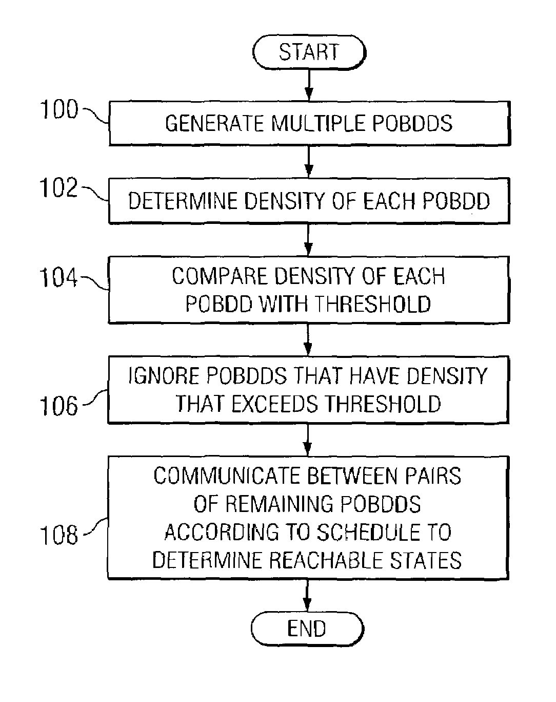
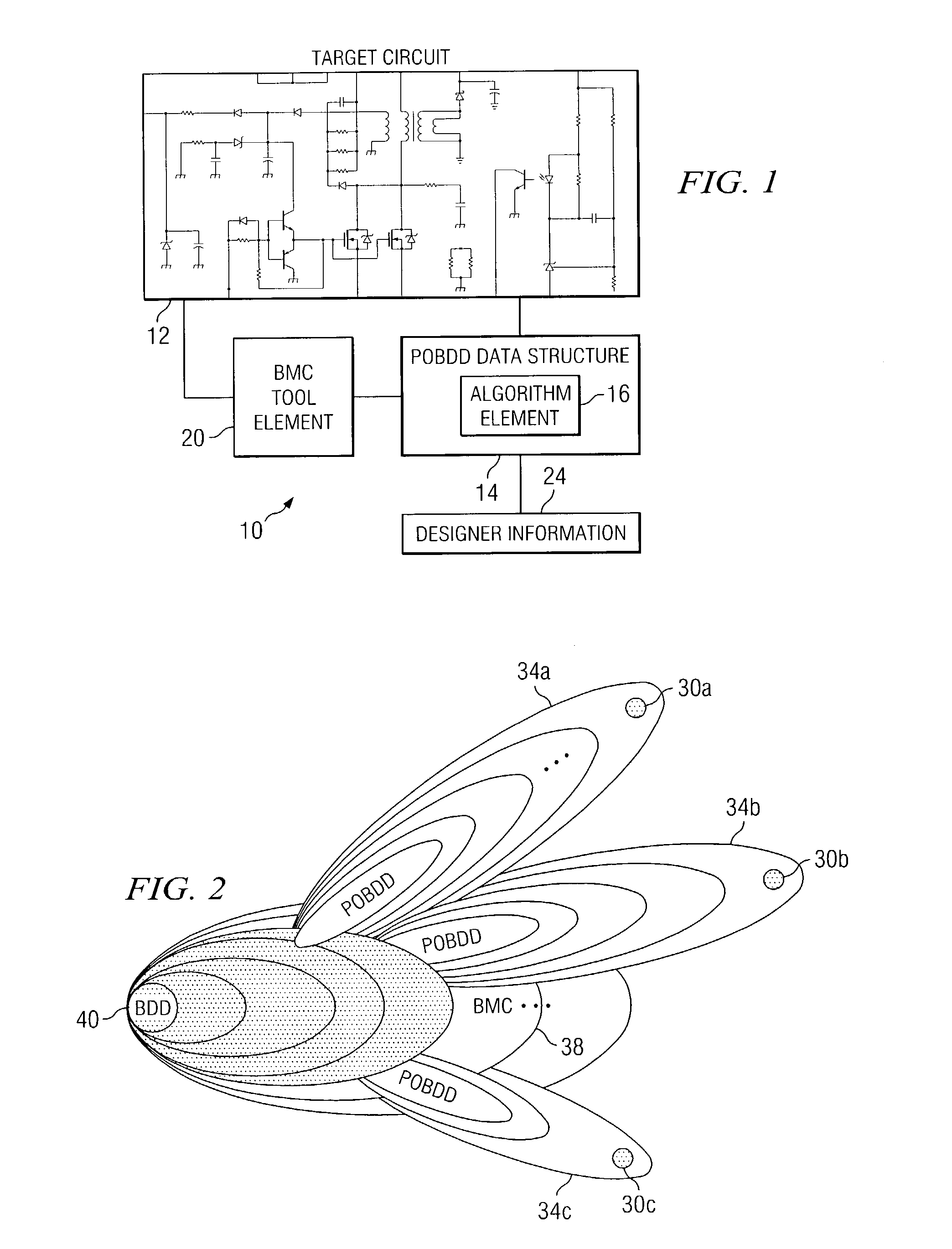
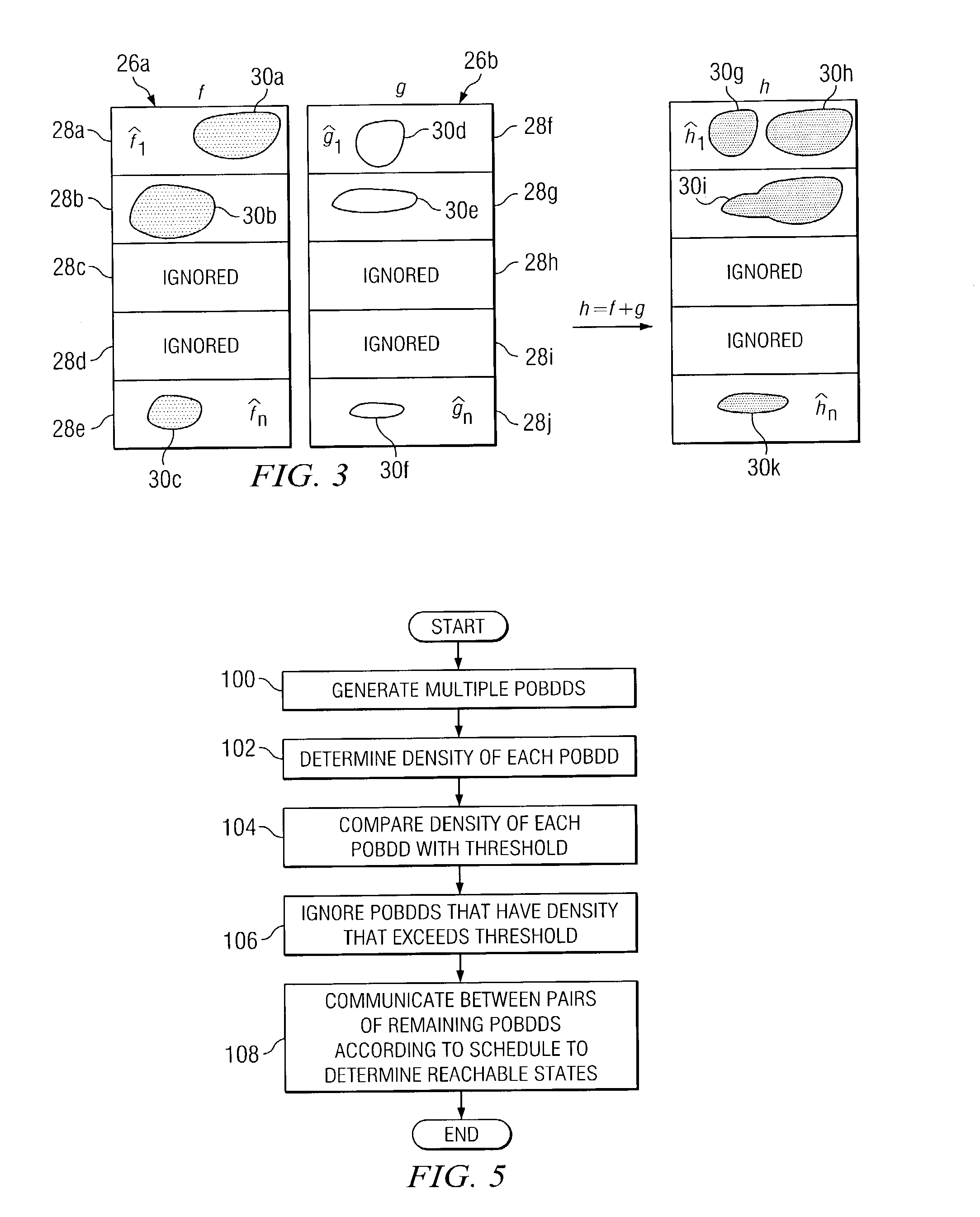
[0016]FIG. 1 illustrates an example system 10 for determining one or more reachable states in a circuit (such as target circuit 12) using one or more partitioned data structures. System 10 may include a partitioned ordered binary decision diagram (POBDD) data structure 14 that includes an algorithm element 16. Additionally, system 10 may include a bounded model checking (BMC) tool element 20 and a segment of designer information 24 that may be communicated to POBDD data structure 14. System 10 may generally be positioned within, or otherwise operate in conjunction with, any integrated circuit, digital element, processing configurations, or binary architecture in which verification procedures or processes may be implemented. Additionally, system 10 may be provided in cooperation with any device, component, hardware, software, object, or element associated with digital processing of information or data.

[0017]System 10 operates to provide a verification process capable of reaching sign...


PUM


Abstract

In one embodiment, a system for verifying a circuit using a scheduling technique includes one or more partitioned ordered binary decision diagram (POBDD) modules that collectively generate one or more POBDDs. Each POBDD corresponds to one or more partitions of a state space of the circuit and includes a number of states and a number of nodes in the partition. The system also includes one or more cost metrics modules that collectively determine a processing cost of each of the partitions of each of the POBDDs. The system also includes one or more scheduling modules that collectively schedule processing of the partitions of the POBDDs for semiformal verification of a circuit. The schedule is based, at least in part, on the determined processing costs of the partitions of the POBDDs.

Description

RELATED APPLICATION[0001]This application claims the benefit, under 35 U.S.C. §119(e), of U.S. Provisional Patent Application No. 60 / 426,207, filed Nov. 13, 2002, which is incorporated herein by reference.TECHNICAL FIELD OF THE INVENTION[0002]This invention relates in general to the field of circuit verification and more particularly to circuit verification.BACKGROUND OF THE INVENTION[0003]The proliferation of integrated circuits (ICs) has placed increasing demands on the design of digital systems included in many devices, components, and architectures. The number of digital systems that include ICs continues to steadily increase and may be driven by a wide array of products and systems. Added functionalities may be implemented in ICs in order to execute additional tasks or to effectuate more sophisticated operations in their respective applications or environments. Additionally, system parameters of ICs may dictate that their operations be performed in an optimal time interval, whi...

Claims


Application Information

Patent Timeline
Patent Type & Authority Patents(United States)
IPC IPC(8): G06F9/45G06F17/50G01R31/28
CPCG06F17/504G06F30/3323
Inventor JAIN, JAWAHARIYER, SUBRAMANIAN K.NARAYAN, AMITSAHOO, DEBASHISSTANGIER, CHRISTIAN
Owner FUJITSU LTD
Why Eureka
Try Eureka