Semiconductor device and method of manufacturing the same, circuit board, and electronic instrument

a semiconductor and semiconductor technology, applied in the direction of semiconductor devices, semiconductor/solid-state device details, electrical apparatus, etc., can solve the problem of difficult to prevent the projecting portion of the penetrating electrode from being contaminated by etching gas

Inactive Publication Date: 2006-04-18
ADVANCED INTERCONNECT SYST LTD
View PDF38 Cites 84 Cited by
  • Summary
  • Abstract
  • Description
  • Claims
  • Application Information

AI Technical Summary

Problems solved by technology

In this case, it is difficult to prevent the projecting portion of t

Method used


Image

  • Semiconductor device and method of manufacturing the same, circuit board, and electronic instrument
  • Semiconductor device and method of manufacturing the same, circuit board, and electronic instrument
  • Semiconductor device and method of manufacturing the same, circuit board, and electronic instrument

Examples


first embodiment

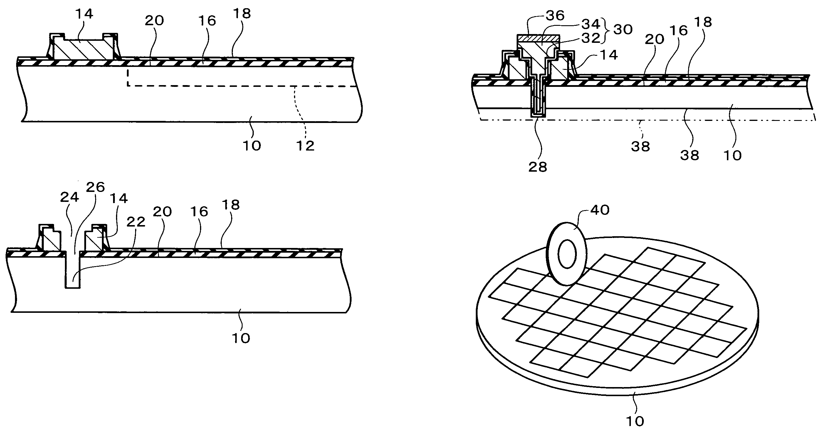
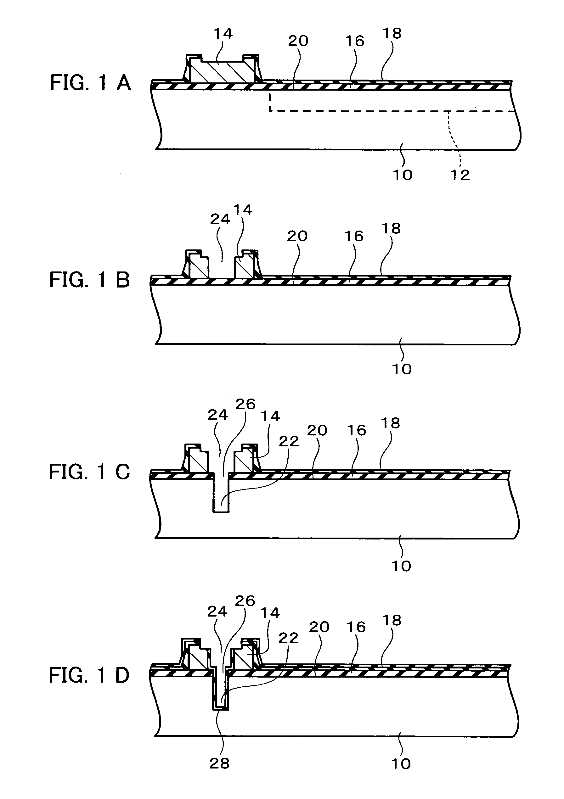
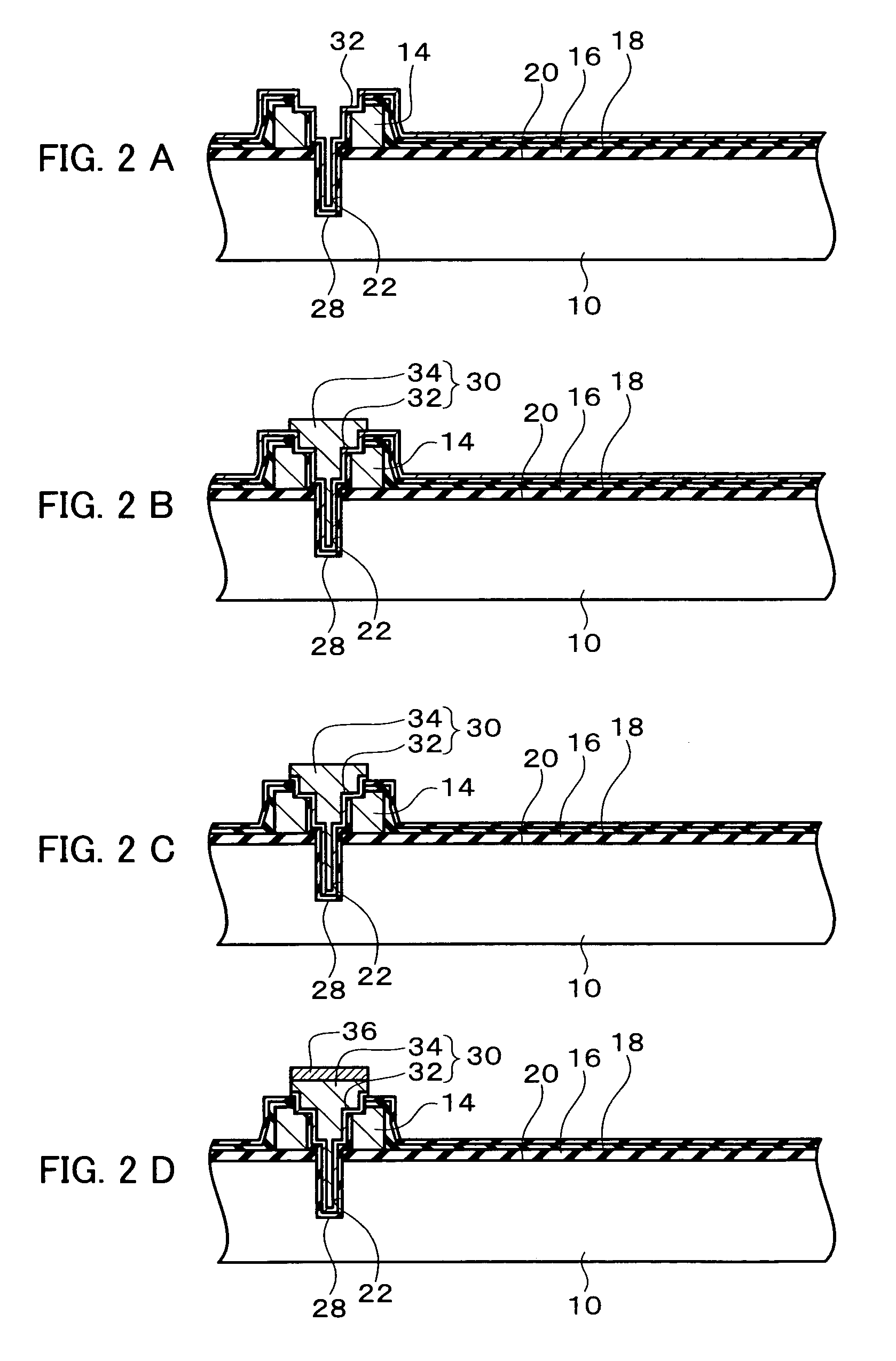
[0086]FIGS. 1A to 3C are diagrams for illustrating a method of manufacturing a semiconductor device according to a first embodiment of the present invention. In this embodiment, a semiconductor substrate 10 is used. The semiconductor substrate 10 shown in FIG. 1A is a semiconductor wafer, but it may be a semiconductor chip. On the semiconductor substrate 10 is formed at least one (a plurality on a semiconductor wafer; one on a semiconductor chip) integrated circuit (for example, a circuit comprising transistors or memory) 12. On the semiconductor substrate 10 are formed a plurality of electrodes (for example, pads) 14. Each electrode 14 is electrically connected to the integrated circuit 12. The electrodes 14 may be formed of aluminum. The surface form of the electrodes 14 is not particularly restricted, but is commonly rectangular. When the semiconductor substrate 10 is a semiconductor wafer, in each of the regions for the plurality of semiconductor chips, two or more (one group of...

second embodiment

[0104]FIGS. 9A to 9C are diagrams for illustrating a method of manufacturing a semiconductor device according to a second embodiment of the present invention. In this embodiment, a groove 100 is formed in the semiconductor substrate 10 (more precisely, in the first surface 20 thereof). The groove 100 is formed along the cutting line of the semiconductor substrate 10. The groove 100 may be formed by cutting, or may be formed by etching. The groove 100 may be formed in the step of forming the depression 22 shown in FIG. 1C, with the same process (for example, at the same time) as the depression 22. The insulating layer 28 may be provided within the groove 100. The groove 100 may be of substantially the same depth as the depression 22, or may be deeper than the depression 22, or may be shallower than the depression 22.

[0105]Thereafter, the process described in FIGS. 3A to 3C in the first embodiment is carried out. FIGS. 9A to 9C show the configuration in the vicinity of the groove 100 ...

third embodiment

[0108]FIGS. 10A and 10B are diagrams for illustrating a method of manufacturing a semiconductor device according to a third embodiment of the present invention. In this embodiment, as shown in FIG. 10A, the process of removing the bottom portion of the groove 100 is carried out with the material of the semiconductor substrate 10 exposed within the groove 100. For example, after carrying out the process of forming the insulating layer 28 shown in FIG. 1D within the depression 22, the groove 100 may be formed, and in order that the insulating layer 28 is not attached, a resist or the like may be provided within the groove 100, or the insulating layer 28 which has entered the groove 100 may be removed. Other details are as described in the second embodiment.

[0109]In this embodiment, the process of FIG. 3B described in the first embodiment is carried out, and by means of the first etchant, the bottom portion of the groove 100 formed by a part of the semiconductor substrate 10 is etched ...


PUM


Abstract

A depression is formed from a first surface of a semiconductor substrate. An insulating layer is provided on the bottom surface and an inner wall surface of the depression. A conductive portion is provided inside the insulating layer. A second surface of the semiconductor substrate is etched by a first etchant having characteristics such that the etching amount with respect to the semiconductor substrate is greater than the etching amount with respect to the insulating layer, and the conductive portion is caused to project while covered by the insulating layer. At least a portion of the insulating layer formed on the bottom surface of the depression is etched with a second etchant having characteristics such that at least the insulating layer is etched without forming a residue on the conductive portion, to expose the conductive portion.

Description

CROSS REFERENCE TO RELATED APPLICATION[0001]This application is a continuation of International Patent Application No. PCT / JP03 / 03302, having an international filing date of Mar. 19, 2003, which designated the United States, the entirety of which is incorporated herein by reference. Japanese Patent Application No. 2002-76308 filed on Mar. 19, 2002 and Japanese Patent Application No. 2003-7277 filed on Jan. 15, 2003 are also incorporated herein by reference in their entirety.BACKGROUND OF THE INVENTION[0002]The present invention relates to a semiconductor device and method of manufacturing the same, a circuit board, and an electronic instrument.[0003]A semiconductor device for three-dimensional mounting has been developed. It is known to form electrodes penetrating a semiconductor chip, to enable three-dimensional mounting. The penetrating electrodes are formed to project from the semiconductor chip. In the conventionally known method of forming a penetrating electrode, a portion of ...

Claims


Application Information

Patent Timeline
IPC IPC(8): H01L21/00H01L21/44H01L21/46H01L21/48H01L21/50H01L23/52H01L21/306H01L21/3205H01L21/768H01L21/78H01L23/12H01L23/31H01L23/48H01L23/485H01L25/065H01L25/07H01L25/18
CPCH01L21/76898H01L24/13H01L23/481H01L24/02H01L24/10H01L25/0657H01L25/50H01L21/30625H01L21/78H01L23/3114H01L2224/0401H01L2224/13099H01L2225/06513H01L2225/06517H01L2225/06541H01L2924/01004H01L2924/01005H01L2924/01006H01L2924/01013H01L2924/01014H01L2924/01018H01L2924/01027H01L2924/01029H01L2924/01033H01L2924/0105H01L2924/01074H01L2924/01078H01L2924/01082H01L2924/014H01L2924/04953H01L2924/14H01L2924/19043H01L2224/16145Y10S438/977Y10S438/959H01L2924/00H01L24/03H01L24/05H01L24/11H01L2224/05551H01L2224/0557H01L2224/06181H01L2224/13H01L2224/13009H01L2924/12042H01L21/768
Inventor MIYAZAWA, IKUYA
Owner ADVANCED INTERCONNECT SYST LTD
Why Eureka
Try Eureka