System and method for defect identification and location using an optical indicia device

Inactive Publication Date: 2006-04-25
ADVANCED MICRO DEVICES INC
View PDF8 Cites 14 Cited by
  • Summary
  • Abstract
  • Description
  • Claims
  • Application Information

AI Technical Summary

Benefits of technology

[0010]A measuring system and method are provided which overcome or minimize the problems and shortcomings of conventional defect identification systems. The invention includes an optical defect inspection system having an optical measurement device adapted to view a workpiece along an optical path, and an optical indicia device in the optical path, adapted to provide location information to the system or a user. The location information can be used to correlate defect locations identified in a wafer before and after a process step, as well as between two different wafers. In addition, the optical indicia device may further allow the use of field comparison techniques in identifying and locating defects in a blank or unpatterned workpiece, by providing fields in a blank workpiece, which may advantageously be compared by the optical measurement device.
[0011]The indicia device may comprise, for example, a transparent member having a grid or other optical indicia patterned thereon. The workpiece surface may be selectively exposed to the optical measurement device (e.g., an optical microscope) through one or more regions in the transparent member, whereby a coordinate system is provided for quantifying the location of the workpiece being viewed at a given time. The inspection system thus allows a user to easily locate a specific area or region of the workpiece for viewing and other analysis. This system may be advantageously employed in comparing patterned and unpatterned or blank semiconductor wafer workpieces, to determine at which processing step a particular defect occurred. The invention further provides methods of detecting and locating defects in patterned and unpatterned workpieces, whereby an optical indicia device is used to identify and locate defects in a blank workpiece, and to correlate the blank workpiece defects with defects identified in a patterned workpiece. The optical indicia device may further be employed in identifying defects in a blank wafer, to facilitate the use of field comparison techniques to quickly locate defects.
[0012]In accordance with one aspect of the invention, there is provided an optical defect inspection system for identifying and locating defects in a workpiece, comprising an optical measurement device adapted to view the workpiece along an optical path, and an optical indicia device located in the optical path, adapted to provide location information to the system or a user. The optical indicia device may comprise, for example, a transparent member having non-transparent optical indicia (e.g., lines) thereon defining a plurality of transparent fields or regions. This provides a grid or other pattern used for determining the location of one or more features on a workpiece, such as particulate or chemical residue defects. The optical indicia device may be moveable in one or more axis relative to the workpiece and / or the optical microscope, to thereby provide for coarse and fine defect location operation. The optical indicia device may further be adapted to move in and out of the optical path of the microscope, to further facilitate defect identification and location.
[0018]According to another aspect of the invention, there is provided a method for identifying a defect in a blank workpiece in an optical defect inspection system having an optical measurement device adapted to view a workpiece along an optical path and an optical indicia device located in the optical path between the workpiece and the optical measurement device and having a transparent member with non-transparent optical indicia defining a plurality of transparent regions in the optical indicia device along the optical path. The method includes viewing the images of two portions of the workpiece through two of the transparent regions using the optical measurement device, comparing the images of the two portions of the workpiece, and identifying a defect in the workpiece in one of the two portions of the workpiece if there is a difference in the images of the two portions of the workpiece. The method thus allows the use of field comparison techniques to facilitate quick identification of defects in a blank wafer.

Problems solved by technology

In addition to particle defects, chemical defects are problematic and may be caused by improper ingredients or mixture ratios in the photoresist.
In similar fashion, the photoresist development process may also introduce defects into a wafer.
For example, a pattern defect may be caused by a mark or blemish in the mask used in a patterning step.
This may cause a defect that is locationally repeatable, whereby the defect may occur at the same location in wafers patterned using the blemished mask.
Similarly, dirt or marks on an exposing tool lens may cause such locationally repeatable defects in a plurality of wafers processed by the tool.
However, it may be difficult to determine the process step at which a particular defect, whether particulate or chemical, was introduced based on inspection of a single wafer.
However, without prior inspection of the wafer or other quantization of the defects associated with the initial processing steps, it may be difficult to determine the step at which a defect occurred.
Field comparison techniques presume that where one field in such a patterned wafer is different from the rest of the fields, a significant probability exists that a defect exists in that field.
Although a defect caused in one step (e.g., a photoresist deposition step) may be detectable after multi-step processing, such a defect may be difficult or impossible to differentiate from a defect introduced at a later step, based on a single inspection of the wafer.
Consequently, field comparison techniques cannot be easily employed to determine the location of defects identified in a blank wafer.

Method used


Image

  • System and method for defect identification and location using an optical indicia device
  • System and method for defect identification and location using an optical indicia device
  • System and method for defect identification and location using an optical indicia device

Examples


Embodiment Construction

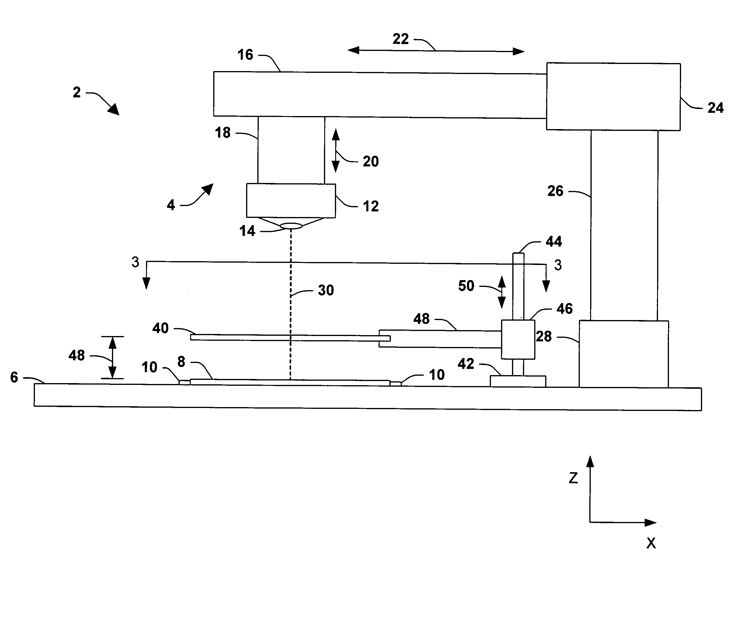
[0030]The following is a detailed description of the present invention made in conjunction with the attached figures, wherein like reference numerals will refer to like elements throughout. The invention provides a system and methods by which workpiece defects and their causes may be identified and located. The invention finds particular application in the field of semiconductor manufacturing. However, it will be recognized that other applications are possible within the scope of the invention. In particular, the various aspects of the invention may be employed to determine which step in a multi-step semiconductor manufacturing process is causing defects in a semiconductor wafer.

[0031]Referring to FIG. 1, an exemplary optical defect inspection system 2 is illustrated having an optical measurement device (e.g., an optical microscope) 4 mounted on a stage 6, and adapted to inspect a workpiece 8 mounted on the stage 6 using retainers 10. The workpiece 8 may include a semiconductor wafe...


PUM


Abstract

A measuring system and method are provided for defect identification and location. The system an optical measurement device adapted to view a workpiece along an optical path, and an optical indicia device located in the optical path between the workpiece and the measurement device, which is adapted to provide location information to the system or a user. The location information can be used to correlate defect locations identified in a wafer before and after a process step, as well as between two different wafers. The optical indicia device may further allow the use of field comparison techniques in identifying and locating defects in a blank or unpatterned workpiece. The indicia device may comprise, for example, a transparent member having a grid or other optical indicia patterned thereon, allowing inspection of the workpiece with reference to the optical indicia pattern.

Description

[0001]The present invention relates generally to measurement instruments used to analyze defects in a semiconductor workpiece, and more particularly to a system and method for optically identifying and locating defects in a semiconductor wafer or other type of workpiece using an optical indicia device.BACKGROUND OF THE INVENTION[0002]In the semiconductor industry there is a continuing trend toward higher device densities. To achieve these high densities there have been, and continue to be, efforts toward scaling down the device dimensions on semiconductor wafers. In order to accomplish such a high device packing density, smaller features sizes are required. This may include the width and spacing of interconnecting lines and the surface geometry such as the corners and edges of various features.[0003]The requirement of small features with close spacing between adjacent features requires high resolution photo lithographic processes as well as high resolution inspection instruments. In...

Claims


Application Information

Patent Timeline
IPC IPC(8): G01N21/88
CPCG01N21/956G01N21/9501
Inventor SUBRAMANIAN, RAMKUMARPHAN, KHOI A.RANGARAJAN, BHARATH
Owner ADVANCED MICRO DEVICES INC
Why Eureka
Try Eureka