Method of manufacturing a superjunction device with conventional terminations

a technology of superjunction device and conventional termination, which is applied in the direction of semiconductor devices, basic electric elements, electrical equipment, etc., can solve the problem of blocking the implantation of the trench

Inactive Publication Date: 2006-05-09
THIRD DIMENSION 3D SEMICON
View PDF41 Cites 48 Cited by
  • Summary
  • Abstract
  • Description
  • Claims
  • Application Information

AI Technical Summary

Benefits of technology

[0009]In a second embodiment of the invention, a method for manufacturing a semiconductor includes providing a semiconductor substrate having first and second main surfaces. The substrate has a heavily doped region of a first conductivity type at the second main surface and a lightly doped region of the first conductivity type at the first main surface. A plurality of trenches and a plurality of mesas are formed in the substrate, each trench having a first portion extending from the first main surface toward the heavily doped region to a first depth position while having a sidewall surface with a pre-determined inclination maintained relative to the first main surface, each one of the plurality being separated from another by a mesa region. In the following step, an oxide deposition is performed to cover the top of each mesa and the sidewalls and bottom of each trench with a thick layer of oxide. The method includes applying a dry oxide etch to remove the oxide on the sidewalls and in the bottom of each trench. Then, a mask is positioned over the trenches and mesas of the preselected area, except for the last trench and a portion of the mesas adjoining the trench. Photoresist is deposited, and the mask removed. The method includes implanting of the selected region of trenches and mesas is performed. However, with the photoresist in place over the last trench, implantation in this trench is blocked. Blocking implantation of the last trench on the opposite end of the structure is accomplished in the same manner. A mask is positioned to allow photoresist to be deposited in the last trench and over a portion of the adjoining mesas, and the mask removed. Implantation in this trench is also blocked by the photoresist. The blocking of implantation of the last trench prevents degradation of the avalanche breakdown voltage of a device formed on this substrate. The photoresist is removed from the trenches and mesas after implantation. After the last trench is cleared, all of the trenches are then filled with an insulating material, and the top surface of the device is planarized. The substrate is then ready for construction of a superjunction device.

Problems solved by technology

However, with the photoresist in place over the last trench, implantation in this trench is blocked.

Method used


Image

  • Method of manufacturing a superjunction device with conventional terminations
  • Method of manufacturing a superjunction device with conventional terminations
  • Method of manufacturing a superjunction device with conventional terminations

Examples


Embodiment Construction

[0029]Certain terminology is used in the following description for convenience only and is not limiting. The words “right”, “left”, “lower”, and “upper” designate directions in the drawing to which reference is made. The words “inwardly” and “outwardly” refer direction toward and away from, respectively, the geometric center of the object described and designated parts thereof. The terminology includes the words above specifically mentioned, derivatives thereof and words of similar import. Additionally, the word “a”, as used in the claims and in the corresponding portions of the specification, means “at least one.”

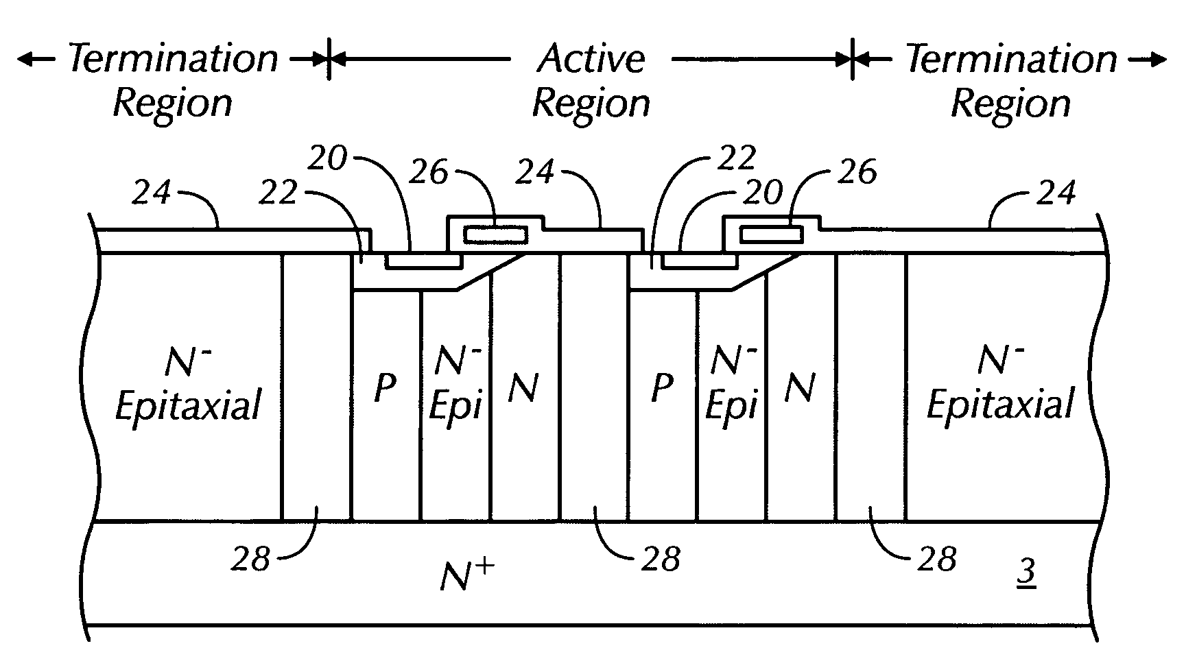
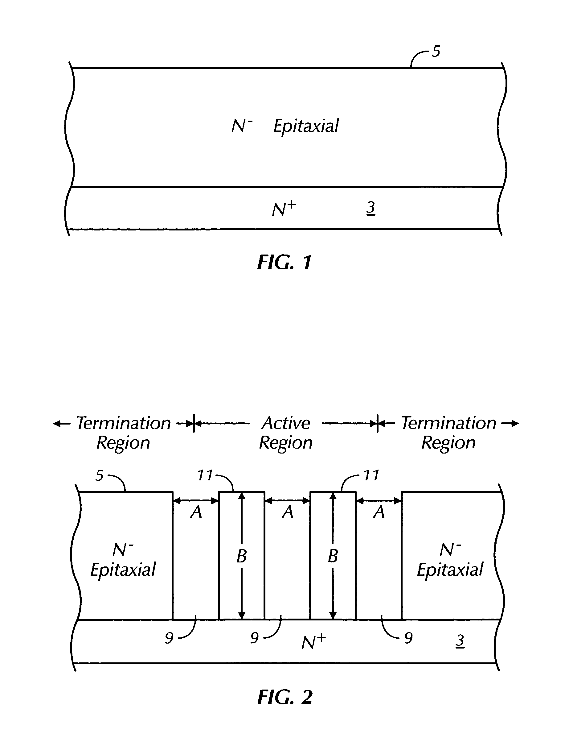
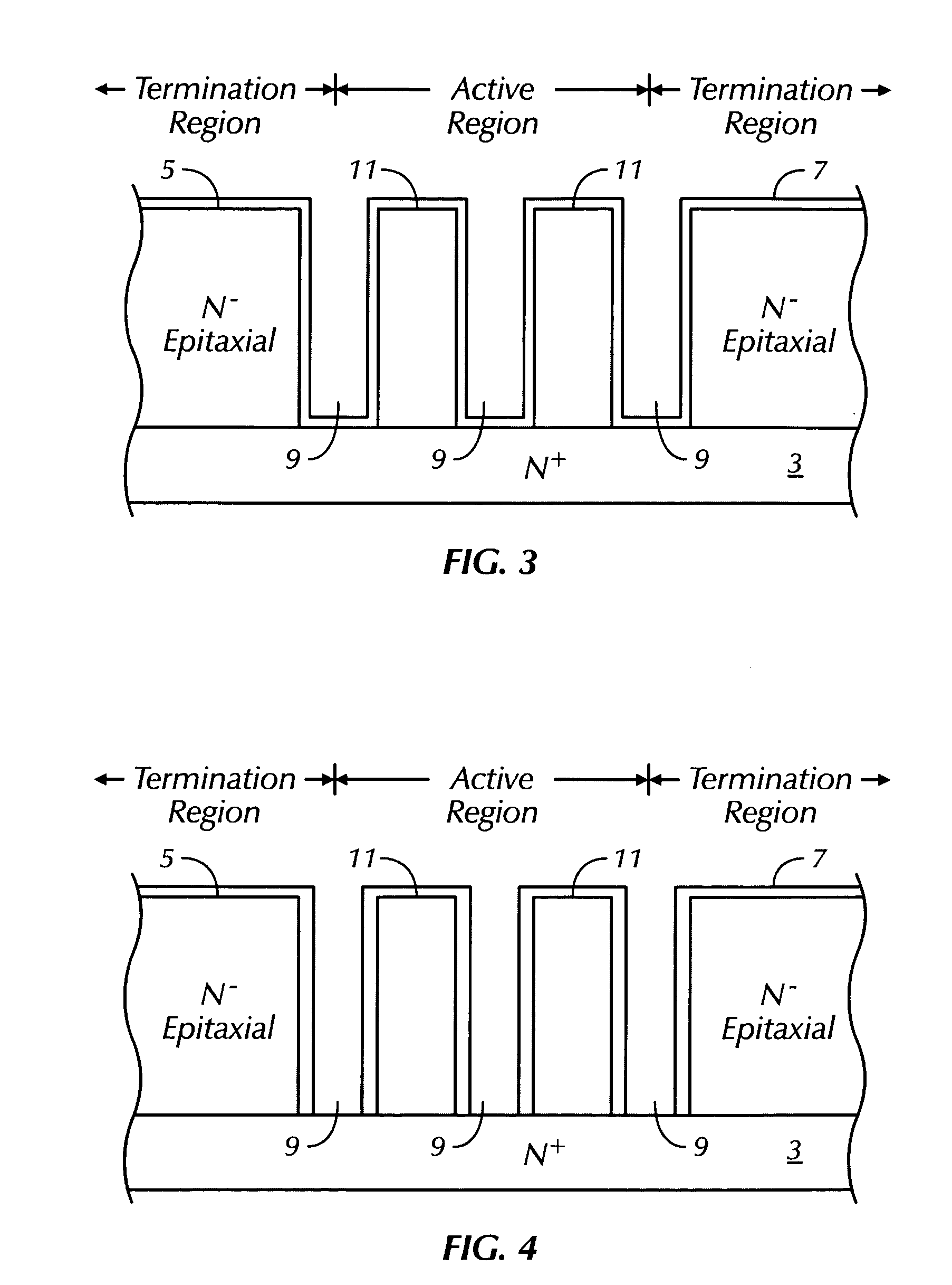
[0030]FIGS. 1–11 generally show a process for manufacturing a superjunction device with conventional terminations in accordance with a first preferred embodiment of the present invention.

[0031]Referring to FIG. 1, there is shown a partial view of a semiconductor wafer that includes a heavily doped N+ substrate 3 and a lightly doped N− layer 5. As used herein, reference to ...


PUM


Abstract

A method of manufacturing a semiconductor device includes providing a semiconductor substrate having a heavily doped region of a first conductivity and has a lightly doped region of the first conductivity. The semiconductor substrate a plurality of trenches etched into an active region of the substrate forming a plurality of mesas. A preselected area in the active region is oxidized and then etched using a dry process oxide etch to remove the oxide in the bottoms of the trenches. A protective shield is formed over a region at a border between the active region and the termination region. The protective shield is partially removed from over the preselected area. Dopants are implanted at an angle into mesas in the preselected area. The plurality of trenches are with an insulating material, the top surface of the structure is planarized and a superjunction device is formed on the structure.

Description

CROSS-REFERENCE TO RELATED APPLICATIONS[0001]This application claims priority to U.S. Provisional Patent Application No. 60 / 531,501, filed Dec. 19, 2003, entitled “Methods of Manufacturing a Superjunction Device with Conventional Terminations.”BACKGROUND OF THE INVENTION[0002]The present invention relates to a method for manufacturing a semiconductor device having an edge termination structure that includes a non-implanted outer sidewall of the last trench of the active region, and particularly to a semiconductor device which is metal-oxide semiconductor (MOS)-gated, and that is suitable for power switching, having both a low on-resistance and a high breakdown voltage.[0003]Since the invention of superjunction devices by Dr. Xingbi Chen, as disclosed in U.S. Pat. No. 5,216,275, there have been many attempts to expand and improve on the superjunction effect of his invention. U.S. Pat. Nos. 6,410,958, 6,300,171 and 6,307,246 are examples of such efforts and are incorporated herein by ...

Claims


Application Information

Patent Timeline
Patent Type & Authority Patents(United States)
IPC IPC(8): H01L21/336H01L21/8238H01L21/265H01L21/266H01L29/06H01L29/78H01L29/812
CPCH01L29/0634H01L29/66712H01L29/7802H01L29/7811H01L21/26586H01L21/266H01L29/0653H01L2924/0002H01L2924/00H01L21/823487H01L29/1045
Inventor HSHIEH, FWU-IUAN
Owner THIRD DIMENSION 3D SEMICON
Why Eureka
Try Eureka