Method of fabricating semiconductor memory device and semiconductor memory device fabricated by the method

Inactive Publication Date: 2008-10-09
SAMSUNG ELECTRONICS CO LTD
View PDF11 Cites 11 Cited by
  • Summary
  • Abstract
  • Description
  • Claims
  • Application Information

AI Technical Summary

Benefits of technology

[0009]Embodiments of the present invention provide a method for fabricating

Problems solved by technology

In the conventional non-volatile semiconductor memory device, a leakage current can be generated due to

Method used


Image

  • Method of fabricating semiconductor memory device and semiconductor memory device fabricated by the method
  • Method of fabricating semiconductor memory device and semiconductor memory device fabricated by the method
  • Method of fabricating semiconductor memory device and semiconductor memory device fabricated by the method

Examples


Embodiment Construction

[0042]Advantages and features of the embodiments of the present invention and methods of accomplishing the same may be understood more readily by reference to the following detailed description of preferred embodiments and the accompanying drawings. The present invention may, however, be embodied in many different forms and should not be construed as being limited to the embodiments set forth herein. Rather, these embodiments are provided so that this disclosure will be thorough and complete and will fully convey the concept of the invention to those skilled in the art. Like reference numerals refer to like elements throughout the specification.

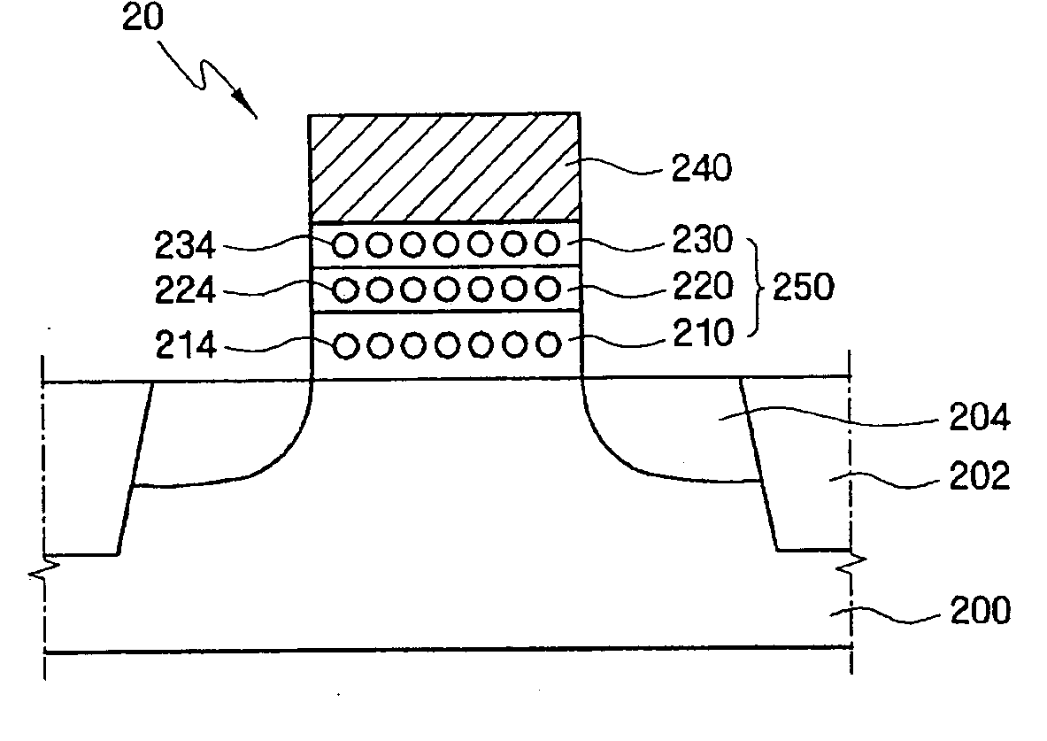
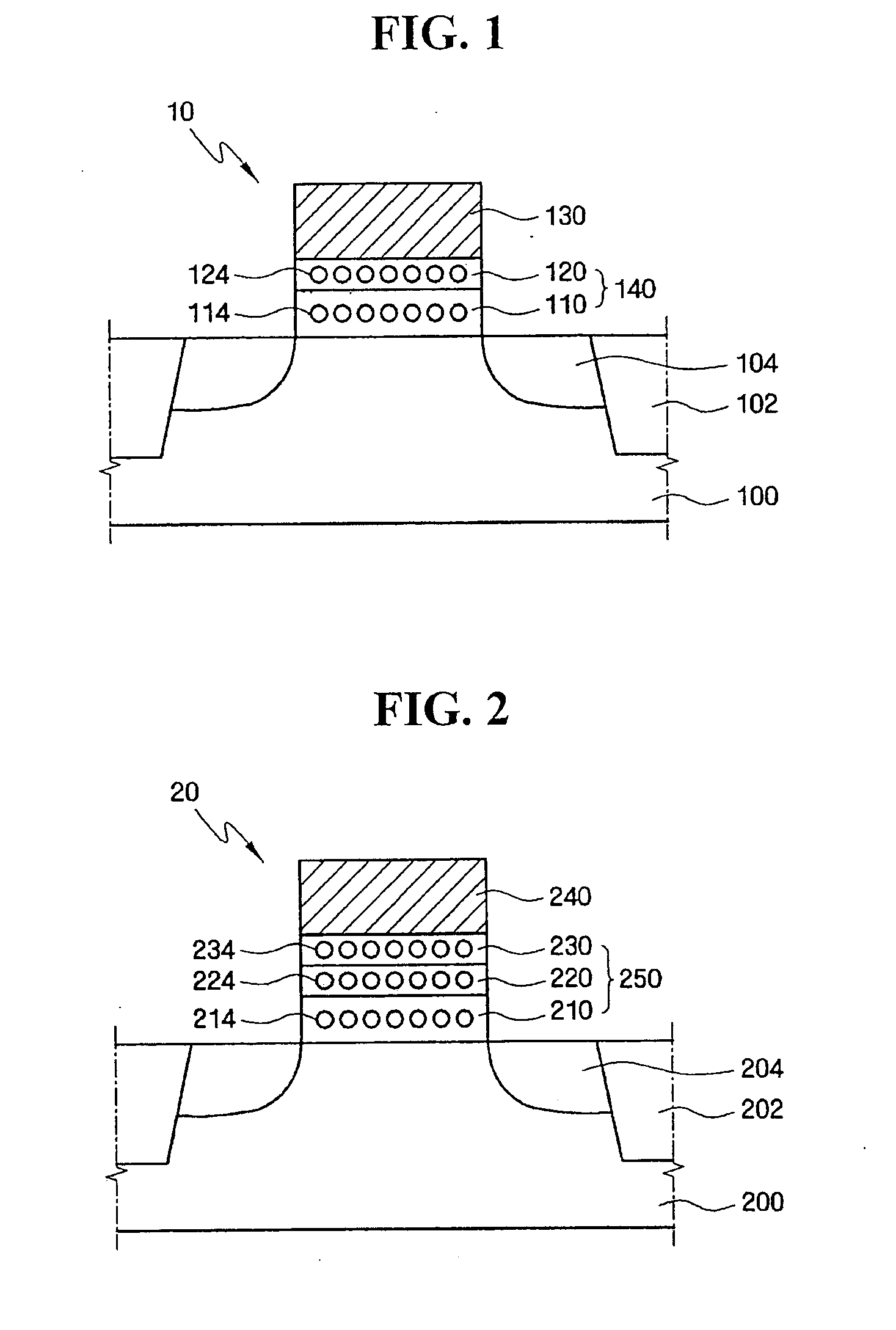
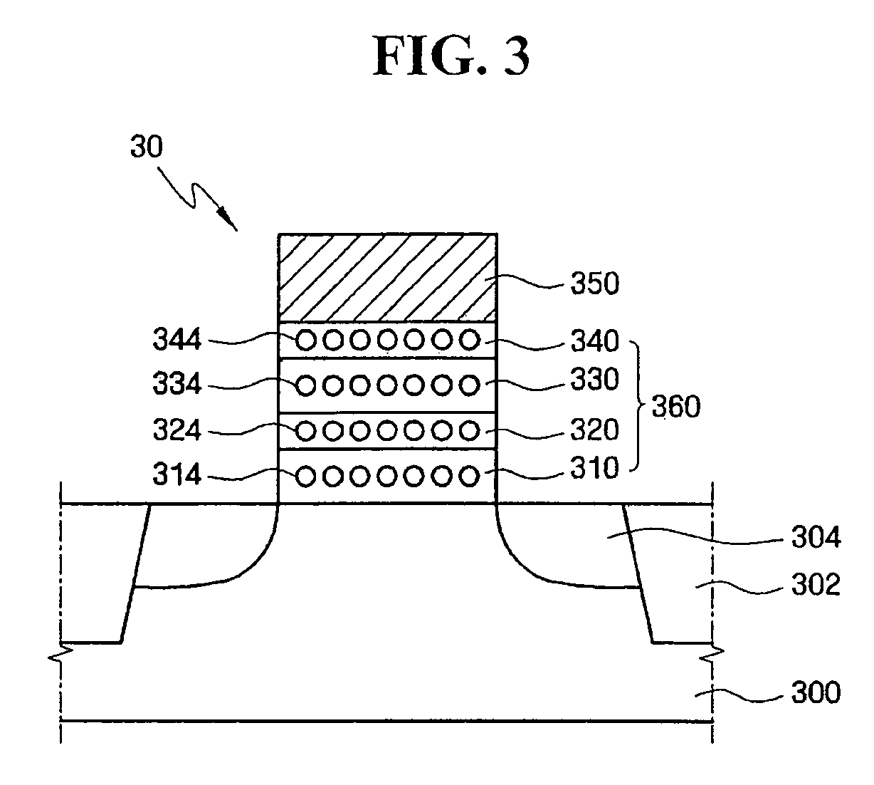
[0043]Structures of semiconductor memory devices according to embodiments of the present invention will first be described with reference to FIGS. 1 through 3. FIGS. 1 through 3 are cross-sectional views of semiconductor memory devices according to embodiments of the present invention.

[0044]As shown in FIGS. 1 through 3, an active region is d...


PUM


Abstract

In a method for fabricating a semiconductor memory device and a semiconductor memory device fabricated by the method, the method includes forming a multi-layered dielectric structure including a first dielectric layer with an ion implantation layer and a second dielectric layer without an ion implantation layer, over a semiconductor substrate; forming nanocrystals in the first and second dielectric layers by diffusing ions of the ion implantation layer by thermally treating the multi-layered dielectric structure; and forming a gate electrode on the multi-layered dielectric structure.

Description

CROSS-REFERENCE TO RELATED APPLICATION[0001]This application claims priority from Korean Patent Application No. 10-2007-0010990 filed on Feb. 2, 2007 in the Korean Intellectual Property Office, the disclosure of which is incorporated herein by reference in its entirety.BACKGROUND OF THE INVENTION[0002]1. Field of the Invention[0003]Embodiments of the present invention relate to a method for fabricating a semiconductor memory device and a semiconductor memory device fabricated by the method, and more particularly, to a method for fabricating a semiconductor memory device containing nanocrystals and a semiconductor memory device fabricated by the method.[0004]2. Description of the Related Art[0005]Semiconductor memory devices can generally be categorized as nonvolatile memory devices and volatile memory devices, depending on the storage state of data. In recent years, nonvolatile memory devices, which maintain data stored therein even if power is interrupted, have enjoyed a dramatic i...

Claims


Application Information

Patent Timeline
IPC IPC(8): H01L27/108H01L21/425
CPCB82Y10/00H01L21/26506H01L21/28273H01L29/42332H01L29/7881H01L29/40114H01L29/66825
Inventor PARK, YOUNG-SOOCHOI, SAM-JONGCHO, KYOO-CHULKANG, TAE-SOO
Owner SAMSUNG ELECTRONICS CO LTD
Why Eureka
Try Eureka