Amorphous etch stop for the anisotropic etching of substrates

a technology of anisotropic etching and amorphous etch stop, which is applied in the direction of basic electric elements, electrical apparatus, semiconductor devices, etc., can solve the problems of inconsistent device structure formation on a substrate, unsatisfactory dummy structure, and electrical interferen

Active Publication Date: 2006-05-16
INTEL CORP
View PDF8 Cites 155 Cited by
  • Summary
  • Abstract
  • Description
  • Claims
  • Application Information

AI Technical Summary

Problems solved by technology

A problem found in etching substrates on which structures have been formed is microloading.
Microloading is a significant problem affecting the performance of integrated circuits because it results in the formation of devices on a substrate that have inconsistent structures as compared to other devices on the same substrate.
Dummy structures are not ideal because they take up space on a substrate that may be put to better use and because large spaces between structures may be needed for specific device requirements.
The drawback to using elements such as boron, phosphorous, and arsenic is that they may diffuse from the etch stop area into regions where they may cause electrical interference with devices formed in or on the substrate.
But, this method requires a number of steps and will not fully prevent the problem of inconsistent undercutting due to microloading and cannot be used when undercutting for structures such as source / drain tip extension regions.

Method used


Image

  • Amorphous etch stop for the anisotropic etching of substrates
  • Amorphous etch stop for the anisotropic etching of substrates
  • Amorphous etch stop for the anisotropic etching of substrates

Examples


Embodiment Construction

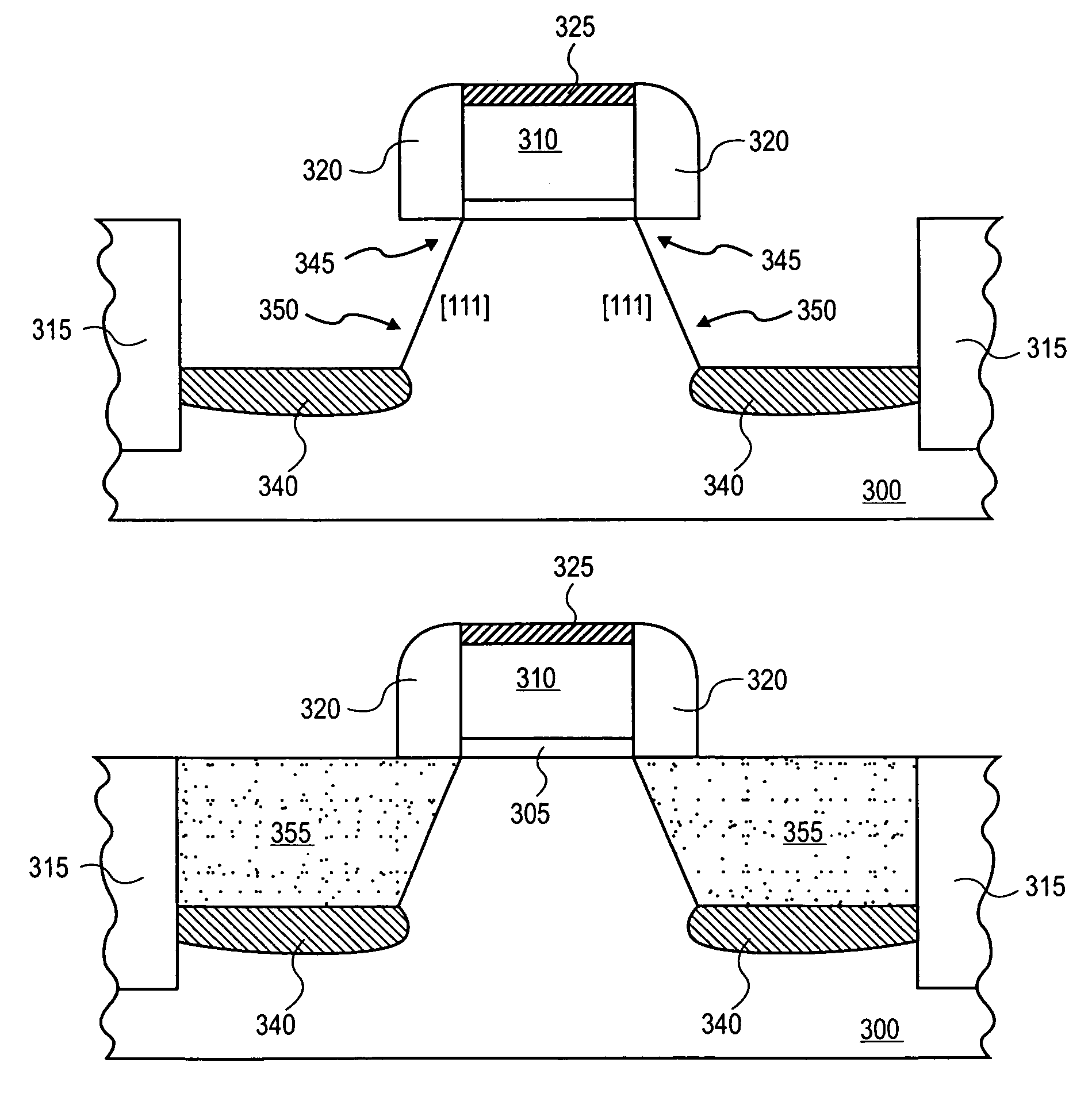
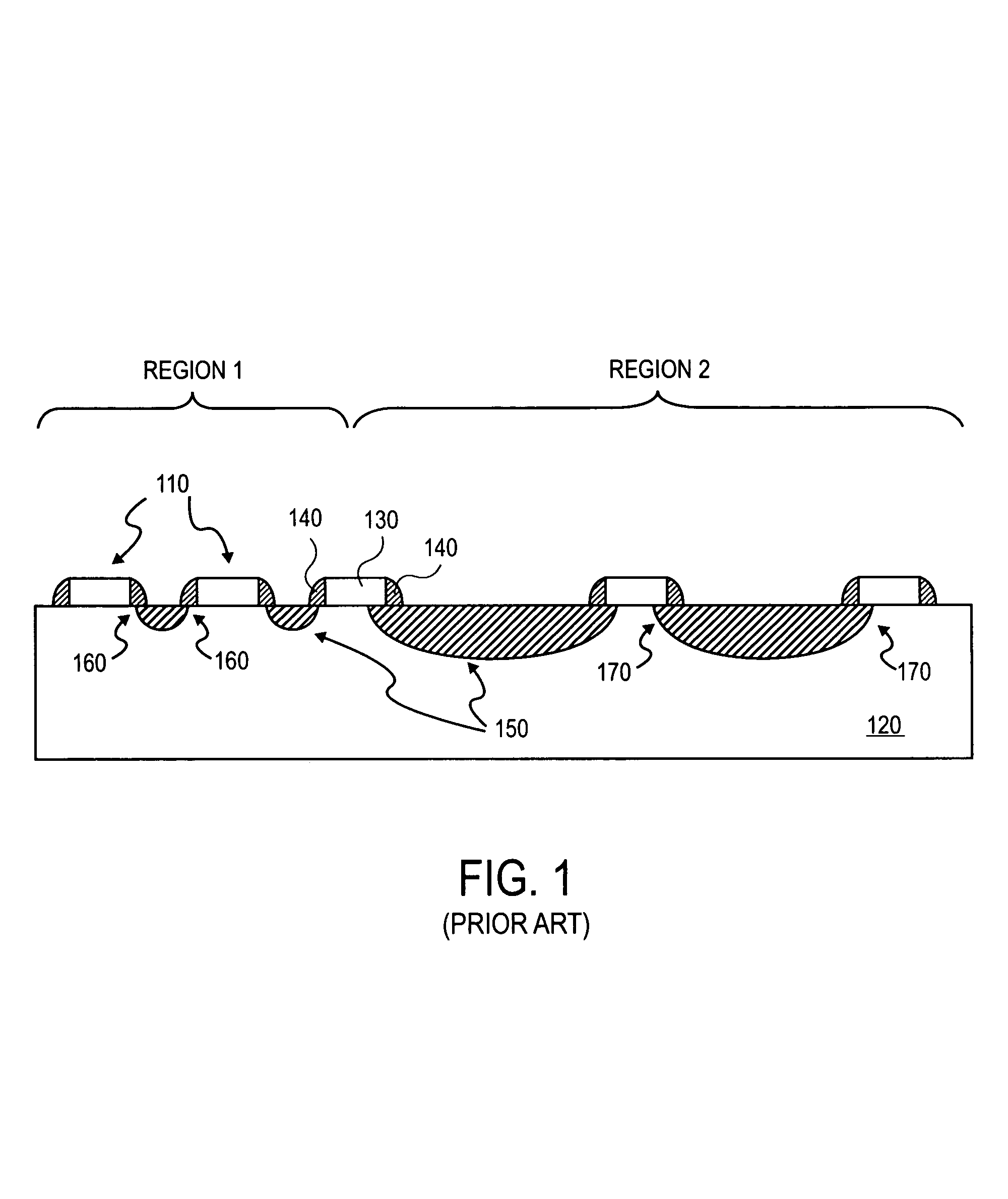
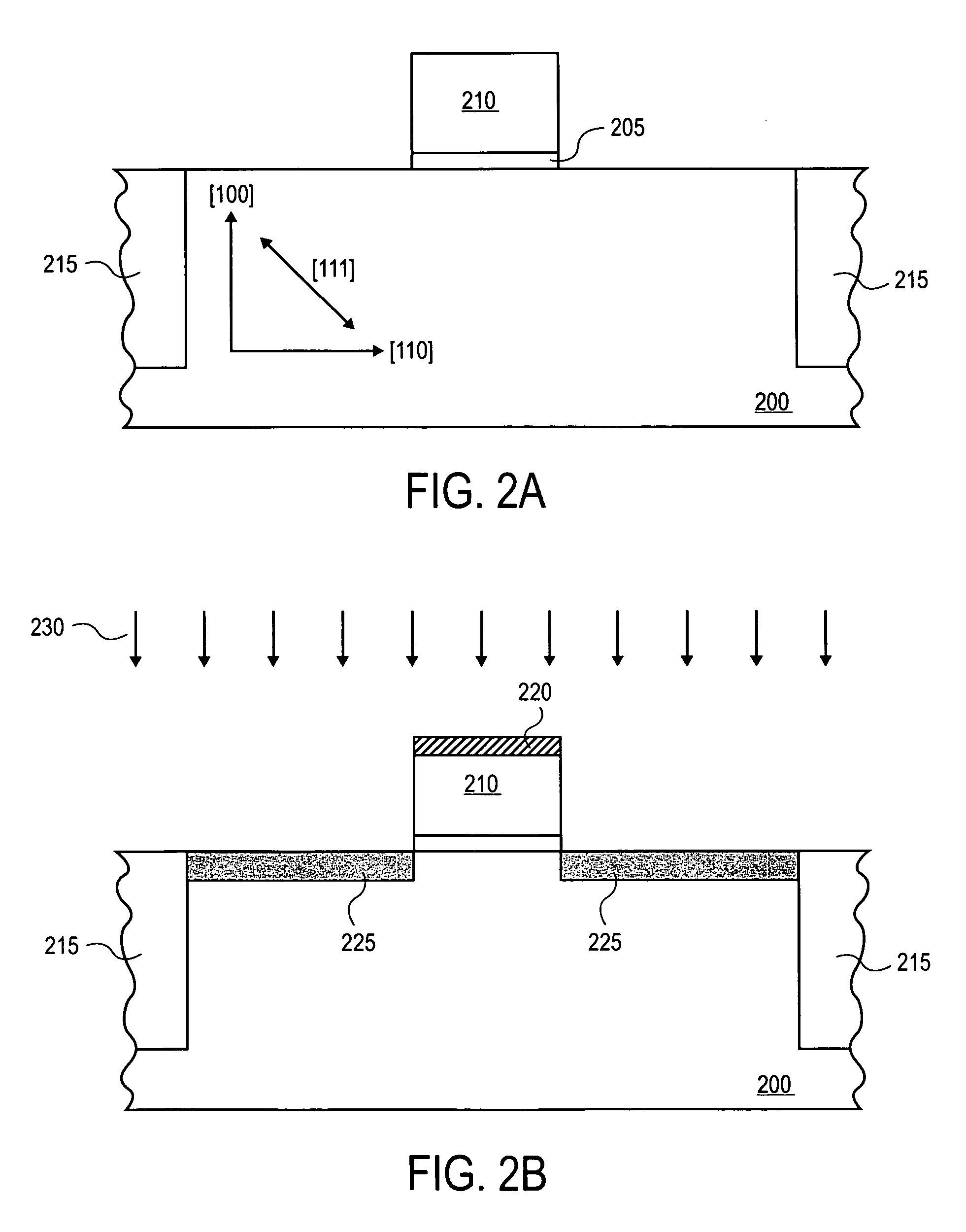
[0012]Described herein are methods and devices employing an amorphous etch stop layer formed by implanting elements that are electrically neutral within a substrate. In the following description numerous specific details are set forth. One of ordinary skill in the art, however, will appreciate that these specific details are not necessary to practice embodiments of the invention. While certain exemplary embodiments of the invention are described and shown in the accompanying drawings, it is to be understood that such embodiments are merely illustrative and not restrictive of the current invention, and that this invention is not restricted to the specific constructions and arrangements shown and described because modifications may occur to those ordinarily skilled in the art. In other instances, well known semiconductor fabrication processes, techniques, materials, equipment, etc., have not been set forth in particular detail in order to not unnecessarily obscure embodiments of the p...


PUM

PropertyMeasurementUnit
depthaaaaaaaaaa
depthaaaaaaaaaa
depthaaaaaaaaaa

Abstract

Methods of forming an amorphous etch stop layer by implanting a substrate with an element that is electrically neutral within the substrate are described. The use of elements that are electrically neutral within the substrate prevents electrical interference by the elements if they diffuse to other areas within the substrate. The amorphous etch stop layer may be used as a hard mask in the fabrication of transistors or other devices such as a cantilever.

Description

BACKGROUND OF THE INVENTION[0001]1. Field of the Invention[0002]The present invention relates to the field of etching substrates for use in integrated circuits, and more particularly to the field of anisotropic wet etching and the use of amorphous etch stop regions.[0003]2. Discussion of Related Art[0004]A problem found in etching substrates on which structures have been formed is microloading. Microloading is the influence that the differing densities of structures in different regions on a single substrate will have on the etch geometry in those different regions. Examples of different etch geometries in regions having different structure densities are illustrated in FIG. 1. Region 1 is a region having a relatively high density of structures 110 formed on the substrate 120. The structures 110 used for example in FIG. 1 are transistor gates 130 having sidewall spacers 140. In this example, the substrate is etched to form recesses that are subsequently backfilled with a doped materi...

Claims


Application Information

Patent Timeline
Patent Type & Authority Patents(United States)
IPC IPC(8): H01L21/336H01L21/265H01L21/306H01L21/308H01L29/165
CPCH01L21/30608H01L29/66636H01L21/3086H01L21/3081H01L21/26506H01L29/165H01L21/265H01L21/3063
Inventor KEATING, STEVENAUTH, CHRIS
Owner INTEL CORP
Why Eureka
Try Eureka