

Method for reducing dimensions between patterns on a photoresist
a photoresist and pattern technology, applied in the field of semiconductor device, photomechanical treatment, instruments, etc., can solve the problems of inability to accurately patterned and defined distance separating patterns smaller than the wavelength of light sources, ineffective relative etching resistance of photoresist layers with a lower thickness, etc., to enhance the etching resistance of a patterned photoresist layer and reduce the distance separating patterns
- Summary
- Abstract
- Description
- Claims
- Application Information
AI Technical Summary
Benefits of technology
Problems solved by technology
Method used
Image

Examples
Embodiment Construction
1. Field of the Invention
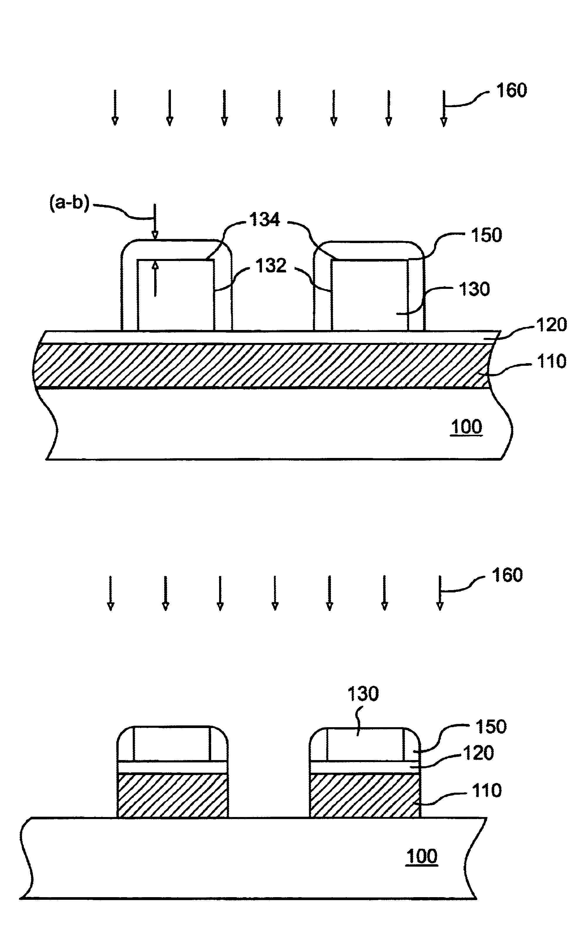
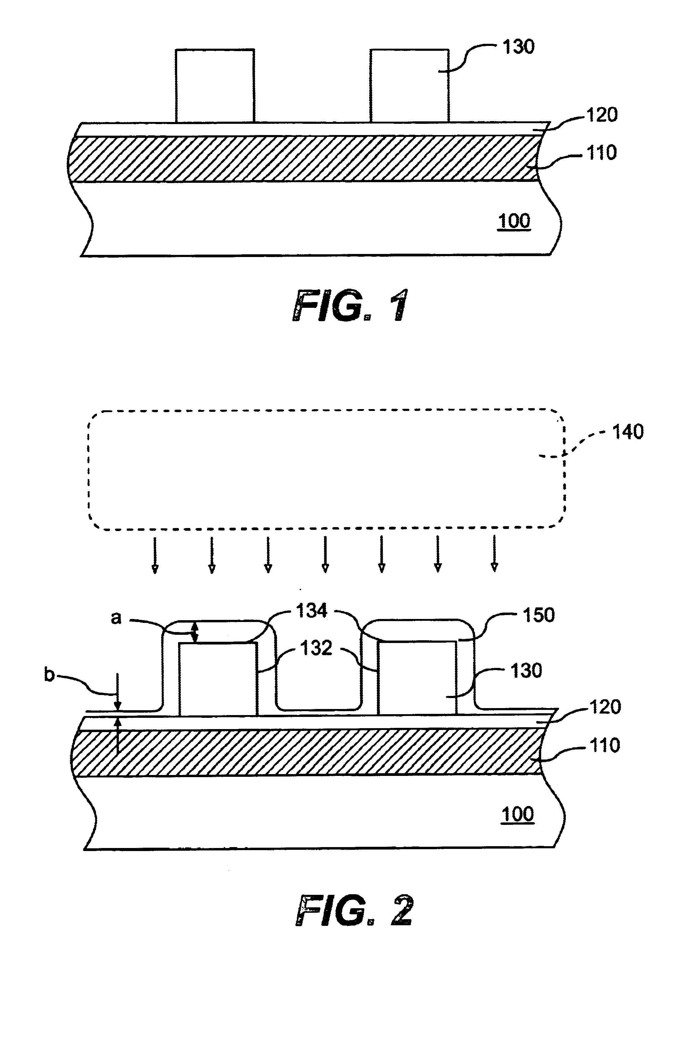
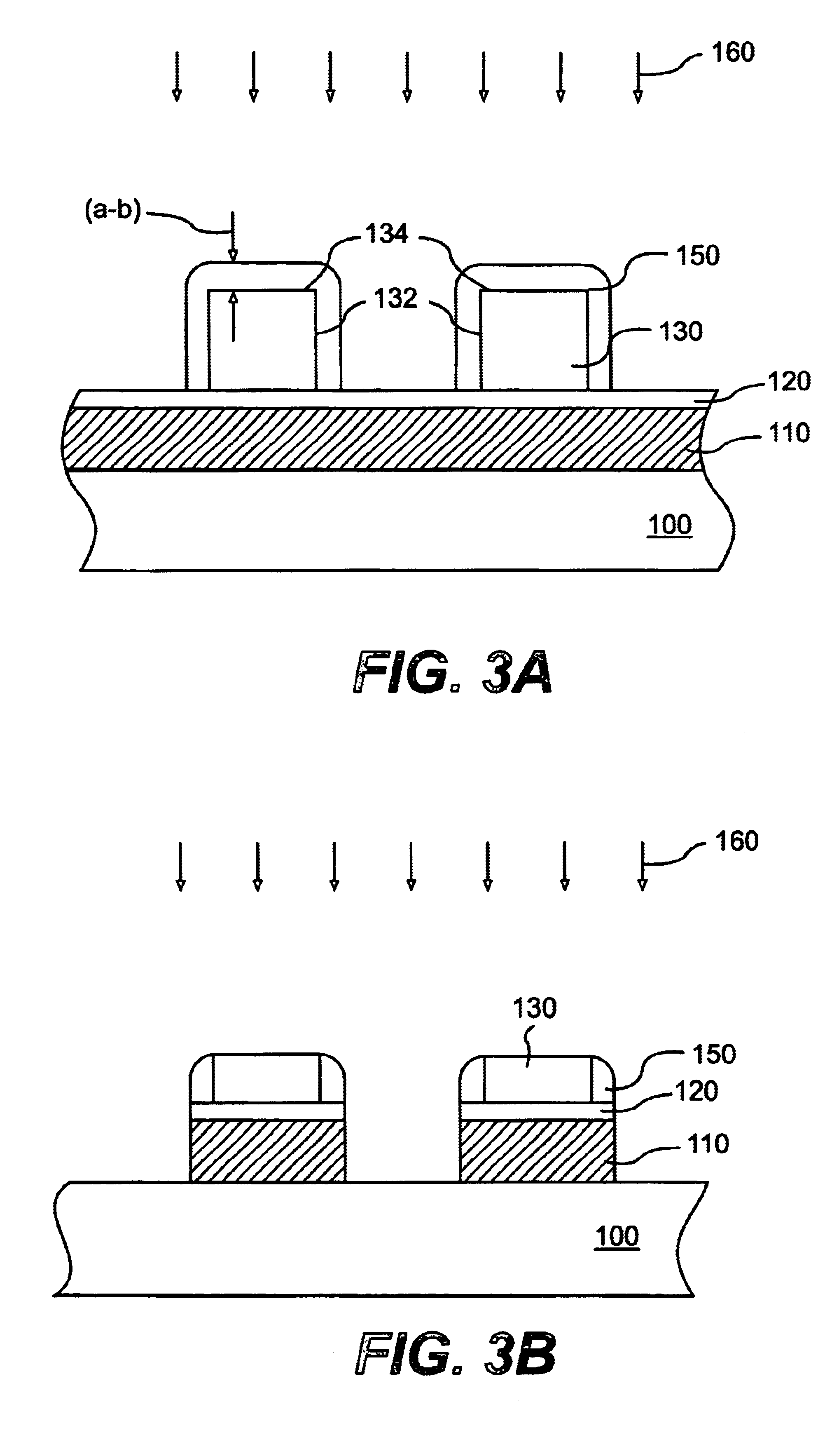
This invention relates in general to a semiconductor manufacturing process and, more particularly, to a photolithographic method having reduced dimensions between patterns on a photoresist.
2. Background of the Invention
With sub-micron semiconductor manufacturing process being the prevalent technology, the demand for a high-resolution photolithographic process has increased. The resolution of a conventional photolithographic method is primarily dependent upon the wavelength of a light source, which dictates that there be a certain fixed distance between patterns on a photoresist. Distance separating patterns smaller than the wavelength of the light source could not be accurately patterned and defined.
Prior art light sources with lower wavelengths are normally used in a high-resolution photolithographic process. In addition, the depth of focus of a high-resolution photolithographic process is shallower compared to a relative low-resolution photolithographic pr...
PUM
| Property | Measurement | Unit |
|---|---|---|
| pressure | aaaaa | aaaaa |
| pressure | aaaaa | aaaaa |
| anisotropic | aaaaa | aaaaa |
Abstract
Description
Claims
Application Information