Self-aligned conductive spacer process for sidewall control gate of high-speed random access memory

a technology of random access memory and sidewall control gate, which is applied in the direction of basic electric elements, electrical equipment, semiconductor devices, etc., can solve the problems of increasing the size of memory cells, not well controlling the dimensions and profiles of sidewall control gates to facilitate proper device design, and the polysilicon etch process

Inactive Publication Date: 2007-02-13
TAIWAN SEMICON MFG CO LTD
View PDF2 Cites 60 Cited by
  • Summary
  • Abstract
  • Description
  • Claims
  • Application Information

AI Technical Summary

Benefits of technology

[0006]In one aspect, the present invention provides a conductive spacer process including the following steps. A floating gate is formed on a semiconductor substrate, and a dielectric layer is then formed on the semiconductor substrate to cover sidewalls of the floating gate. A conductive layer is formed on the dielectric layer, and then an oxide spacer is formed on the conductive layer and located adjacent to the sidewalls of the floating gate. Performing an anisotropic etch process on the conductive layer and using the oxide spacer as a hard mask, a conductive spacer is formed adjacent to the sidewalls of the floating gate, serving as a sidewall control gate.

Problems solved by technology

The conventional anisotropic polysilicon etch process, however, can not well control the dimensions and profiles of the sidewall control gates to facilitate proper device design.
The variation in the spacer width is also unfavorable to subsequent contact process, and therefore an additional polysilicon line is needed for the contact formation, which leads to increase in memory cell size and difficulty in layout design.
Moreover, the anisotropic etch back may round corners of the polysilicon spacers, thus a subsequent silicidation process, for reducing the RC time constant and improving operations of reading, programming, and erasing, can not be perfectly performed in the rounded-shaped control gates.

Method used


Image

  • Self-aligned conductive spacer process for sidewall control gate of high-speed random access memory
  • Self-aligned conductive spacer process for sidewall control gate of high-speed random access memory
  • Self-aligned conductive spacer process for sidewall control gate of high-speed random access memory

Examples


Embodiment Construction

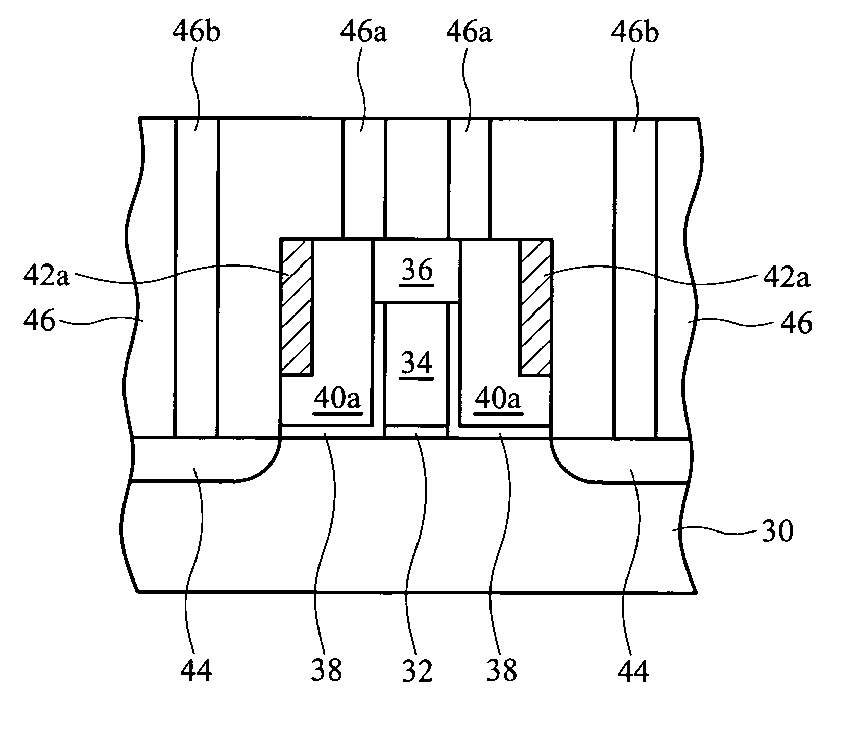
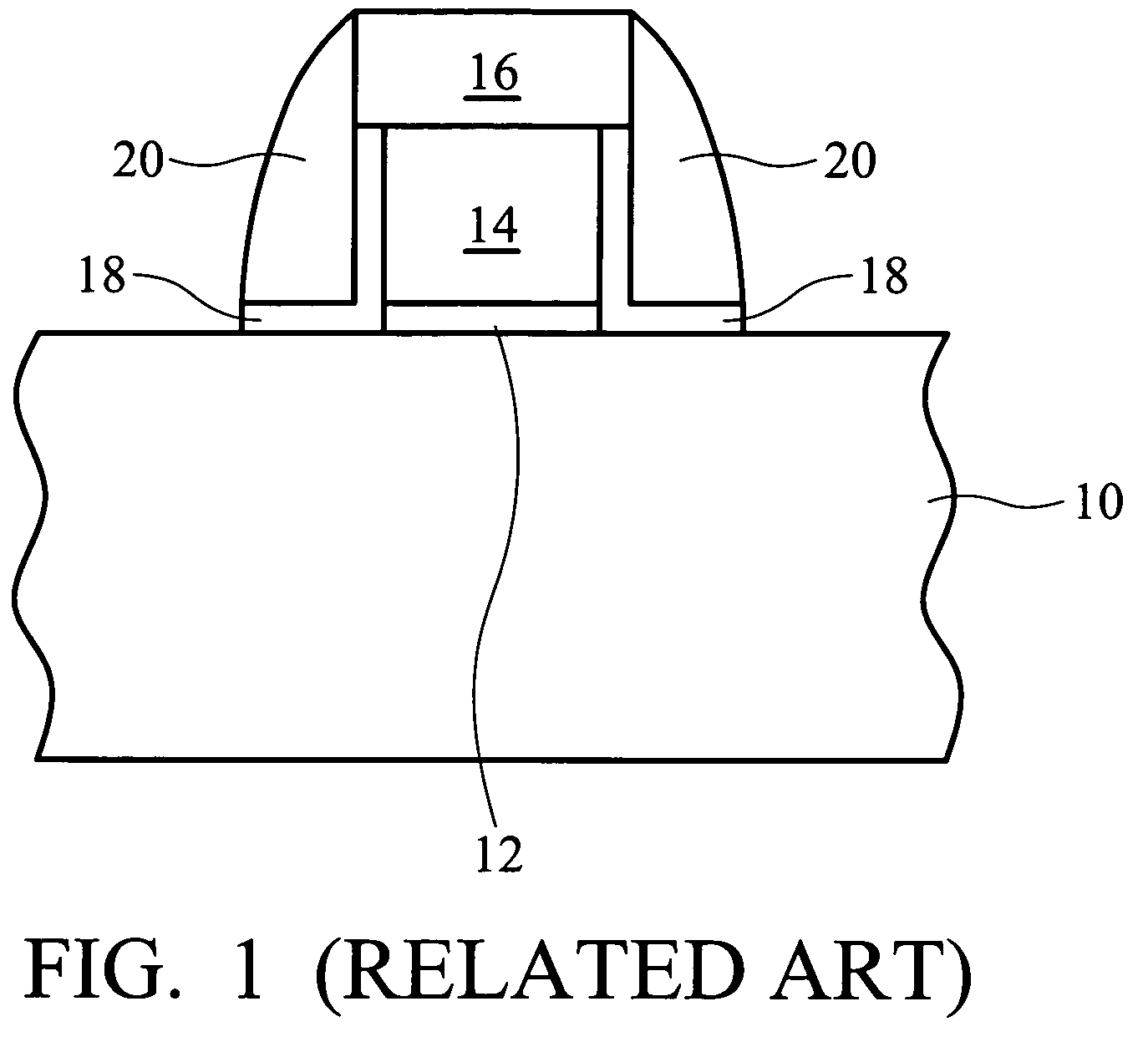
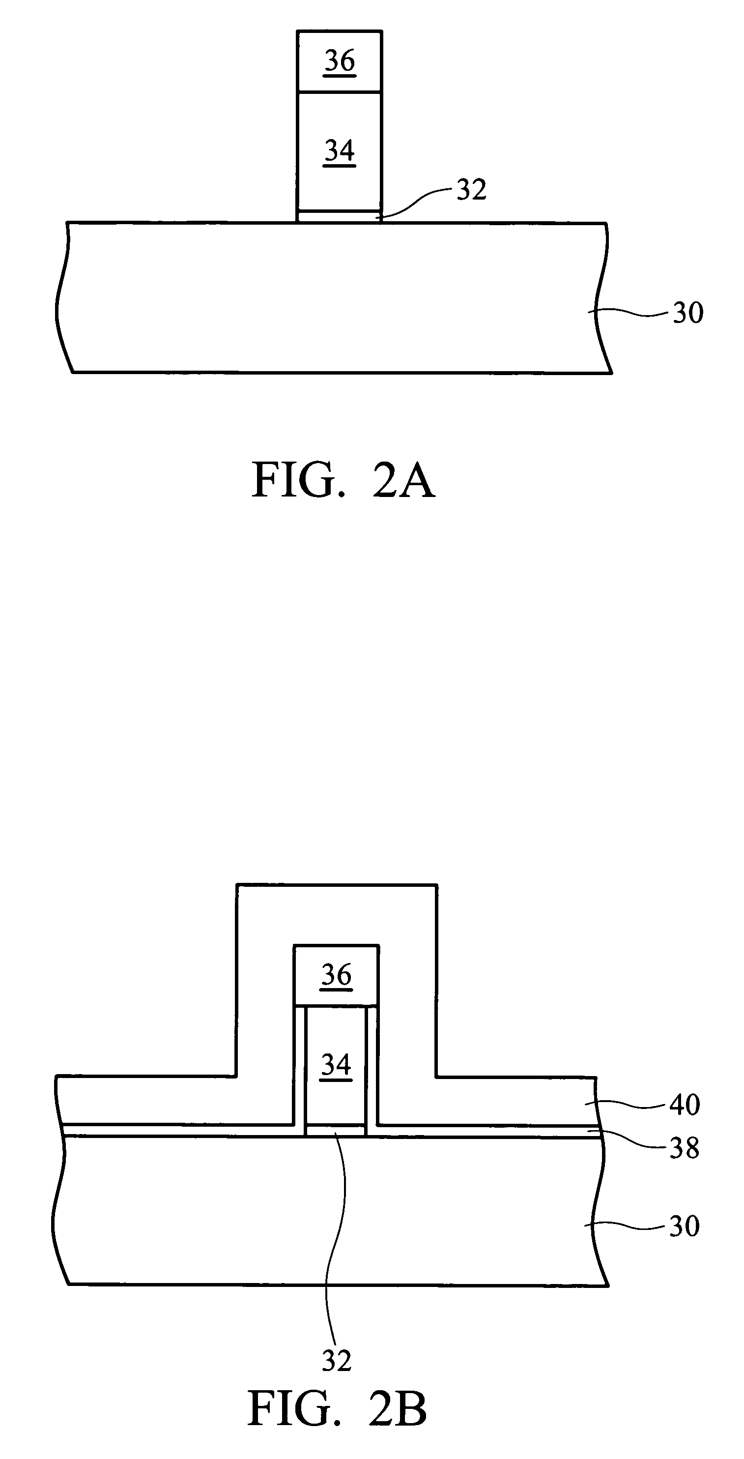
[0012]Embodiments of the present invention provide a self-aligned conductive spacer process to fabricate sidewall control gates on both sides of a floating gate for high-speed RAM applications, which can well define dimensions and profiles of the conductive spacers to form the control gates of an uniform width in a wafer or from wafer to wafer. Thus in subsequent processes, borderless contact formation and silicide formation can be well performed on the self-aligned control gates. Particularly, embodiments of the present invention provide a self-aligned polysilicon spacer process using a polyoxide spacer as an etch back mask to well define the width, thickness and shape of the sidewall control gate. Embodiments of the self-aligned conductive spacer process are simple and fully compatible with the existing CMOS logic technology.

[0013]Reference will now be made in detail to the present embodiments, examples of which are illustrated in the accompanying drawings. Wherever possible, the ...


PUM


Abstract

A self-aligned conductive spacer process for fabricating sidewall control gates on both sides of a floating gate for high-speed RAM applications, which can well define dimensions and profiles of the sidewall control gates. A conductive layer is formed on the dielectric layer to cover a floating gate patterned on a semiconductor substrate. Oxide spacer are formed on the conductive layer adjacent to the sidewalls of the floating gate. Performing an anisotropic etch process on the conductive layer and using the oxide spacers as a hard mask, a conductive spacers are self-aligned fabricated at both sides of the floating gate, serving as sidewall control gates.

Description

TECHNICAL FIELD[0001]The present invention relates to high-speed random access memory (RAM) applications, and particularly to a self-aligned conductive spacer process for fabrication sidewall control gates.BACKGROUND[0002]The demands for highly efficient digital equipment continue to increase, and there is strong need to embed high-speed and low-power-consumption memory into SoC (system-on-chip). Since conventional memories such as SRAM, DRAM, and flash are unsuitable choices for these applications, one unique memory, Direct Tunneling Memory (DTM), with ultra-thin tunnel oxide and novel depleted floating gate is developed for cost-effective and scalable embedded RAM applications. The features of the DTM structure include sidewall control gates fabricated on both sides of a floating gate, and offset source / drain regions without overlapping the floating gate. Its simple fabrication process is fully compatible with the existing CMOS logic technology, and its simple structure can obtain...

Claims


Application Information

Patent Timeline
Patent Type & Authority Patents(United States)
IPC IPC(8): H01L21/336H01L21/302H01L21/3205H01L21/461H01L21/4763H01L21/8234H01L21/8238
CPCH01L29/7881H01L29/42324H01L21/28273H01L21/2815H01L29/40114
Inventor LEE, TZYH-CHEANGYANG, FU-LIANGHWANG, JIUNN-RENLEE, TSUNG-LIN
Owner TAIWAN SEMICON MFG CO LTD
Why Eureka
Try Eureka