CMOS SRAM cell configured using multiple-gate transistors

a technology of multiple gate transistors and sram cells, which is applied in the direction of semiconductor devices, semiconductor/solid-state device details, electrical apparatus, etc., can solve the problems of inability of the gate to substantially control the on and off state of the channel, the size and the desired beta ratio limit the size of the device, and the difficulty of writing the cell into a different state. achieve high permittivity and high permittivity

Inactive Publication Date: 2005-03-08
TAIWAN SEMICON MFG CO LTD
View PDF7 Cites 100 Cited by
  • Summary
  • Abstract
  • Description
  • Claims
  • Application Information

AI Technical Summary

Benefits of technology

The present invention is further directed to an array of static random access memory cells formed by a plurality of SRAM cells arranged in an n by m matrix, wherein n and m are integers greater than 1, and wherein each SRAM cell includes a pair of P-channel multiple-gate field-effect transistors (P-MGFETs), each of the P-MGFETs has a source connected to a common voltage potential and a gate connected to a drain of the other P-MGFET; a first pair of N-channel multiple-gate field-effect transistors (N-MGFETs), each of the first pair of N-MGFETs has a drain connected to the drain of the respective P-MGFET of the pair of P-MGFETs, a common source connected to ground, and a gate connected to the drain of an opposite P-MGFET of the pair of P-MGFETs; a second pair of N-MGFETs that has a drain respectively connected to a connection linking the respective drain of the N-MGFET of the first pair of N-MGFETs to the drain of the P-MGFET of the pair of P-MGFETs; a pair of complementary bit lines, each of the complementary bit lines respectively connected to the source of the N-MGFET of the second pair of N-MGFETs; a plurality of word lines, each of the word lines connected to the gates of the N-MGFETs of the second pair of N-MGFETS; n pairs of complementary bit lines, each of the n pairs of the complementary bit lines linking respective sources of the N-MGFETs of the second pair of N-MGFETs of each of the SRAM cells to form columns of the array; and m word lines, each of the m word lines linking respective gates of the N-MGFETs of the second pair of N-MGFETs of each SRAM cells to form rows of the array.
In the array of static random access memory cells, the pair of P-channel multiple-gate field-effect transistors are pull-up devices and the first pair of N-channel multiple-gate field-effect transistors are pull-down devices. A first P-MGFET of the pair of P-MGFETs and a first N-MGFET of the first pair of N-MGFETs form a first inverter, and a second P-MGFET of the pair of P-MGFETs and a second N-MGFET of the first pair of N-MGFETs form a second inverter, the first and second inverters are cross-coupled to each other. A conductivity of each of the first pair of N-MGFETs is larger than a conductivity of each of the second pair of N-MGFETs. The P-channel or N-channel multiple-gate field-effect transistors may be double-gate field-effect transistors, or may be triple-gate field-effect transistors, or may be omega field-effect transistors.
In the array of static random access memory cells, each of the P-channel or N-channel multiple-gate field-effect transistors may further include a substrate that has an insulating layer on a top surface; at least one semiconductor fin formed vertically on the top surface of the substrate, each fin has a top surface and two sidewall surfaces; a gate dielectric layer overlying the at least one semiconductor fin; a gate electrode wrapping around the at least one semiconductor fin on the top surface and the two sidewall surfaces overlying the gate dielectric layer; and source and drain regions separated by the gate electrode. The at least one semiconductor fin may be at least two semiconductor fins, each has a width different than the other. The at least one semiconductor fin may be formed of silicon, or may be formed of silicon and germanium. The insulating layer may include a dielectric material, or may include silicon oxide. The insulating layer may have a thickness between about 20 Å and about 1000 Å. The gate dielectric layer may be formed of silicon oxide, or may be formed of silicon oxynitride, or may be formed of a high permittivity material selected from the group consisting of La2O3, Al2O3 HfO2, HfON and ZrO2. The gate dielectric layer may include a high permittivity material that has a relative permittivity of at least 5. The gate dielectric layer may have a thickness between about 3 Å and about 100 Å. The gate dielectric layer may have a first thickness on the top surface of the fin and a second thickness on the sidewall surfaces of the fin. The first thickness may be different than the second thickness, or the first thickness may be smaller than the second thickness. A thickness of the gate dielectric layer on the top surface of the semiconductor fin may be less than 20 Å. The gate electrode may be formed of polycrystalline silicon, may be formed of polycrystalline silicon germanium, or may be formed of a metal. Each of the first pair of N-MGFETs may include a first number of semiconductor fins, each of the second pair of N-MGFETs may include a second number of semiconductor fins, the first number may be different than the second number. The first pair of N-MGFETs may share a plurality of semiconductor fins with the second pair of N-MGFETs, or the first pair of N-MGFETs and the second pair of N-MGFETs may not share any semiconductor fins.

Problems solved by technology

The more stable the cell the more difficult it will be to write the cell into a different state.
In practice, the cell size and the desired beta ratio limit the size of the devices.
However, as the gate length of the conventional bulk MOSFET is reduced, it suffers from problems related to the inability of the gate to substantially control the on and off states of the channel.
For device scaling well into the sub-30-nm regime, the requirements for body-doping concentration, gate oxide thickness, and source / drain (S / D) doping profiles become increasingly difficult to meet when conventional device structures based on bulk silicon (Si) substrates are employed.
While there is some work on the design and fabrication of multi-gate devices such as the double-gate and triple-gate devices, there is little work on circuits, such as inverter circuits and static random-access memory (SRAM) cells, configured using such devices.
However, the optimization of circuits, such as SRAM cells, incorporating multiple-gate transistors has not been addressed.

Method used


Image

  • CMOS SRAM cell configured using multiple-gate transistors
  • CMOS SRAM cell configured using multiple-gate transistors
  • CMOS SRAM cell configured using multiple-gate transistors

Examples


Embodiment Construction

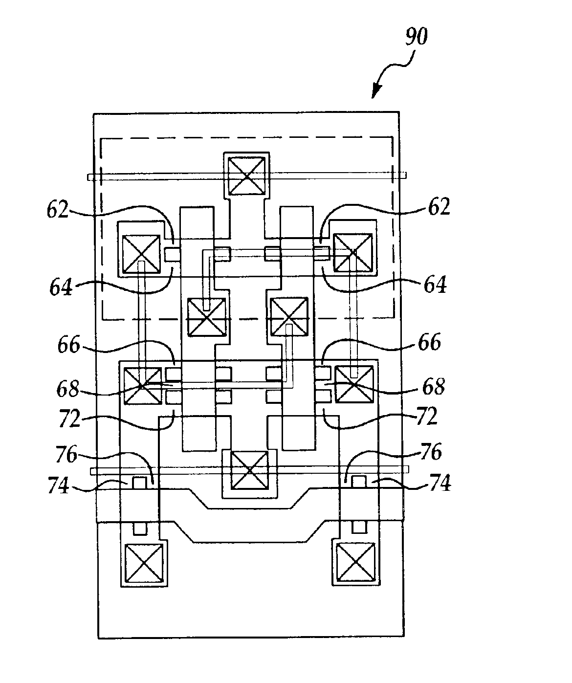
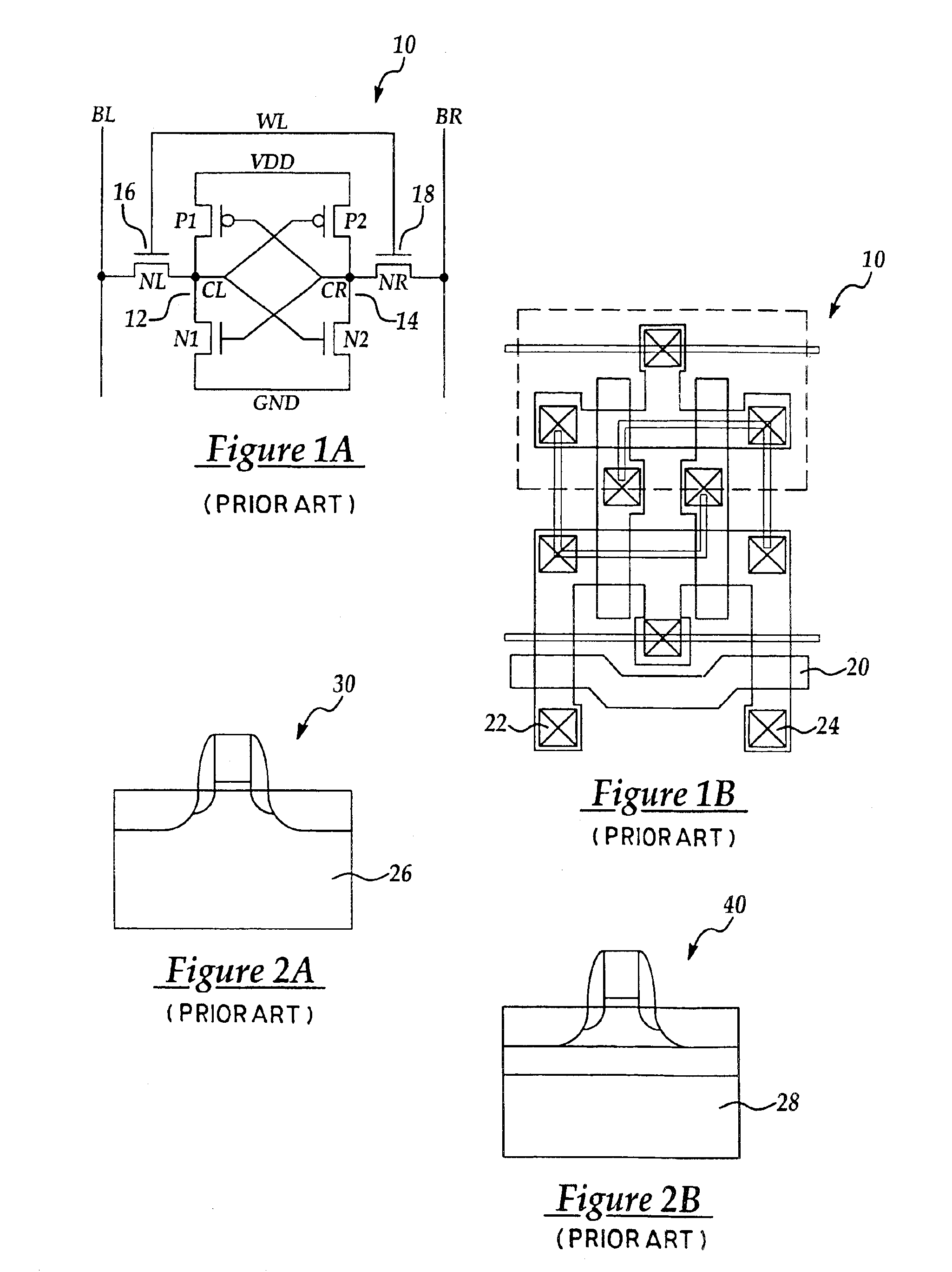
Conventional SRAM cells, an example of which is depicted in FIGS. 1A and 1B are comprised of conventional transistors formed on bulk silicon substrates or silicon-on-insulator substrates. At present, there is no report on the incorporation of multiple-gate field-effect transistors (MGFETS) in an SRAM cell and the optimization of such an SRAM cell.

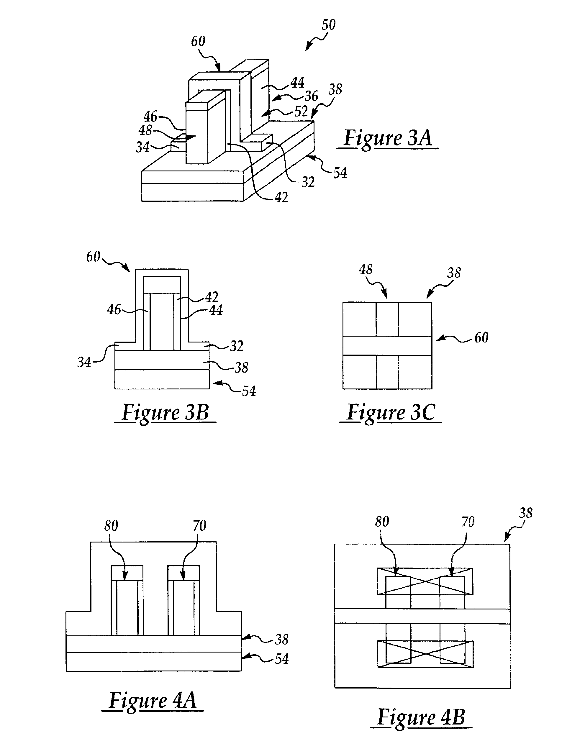
One example of the present invention multiple-gate field-effect transistor is a double-gate field-effect transistor (FET) structure 50, shown in FIGS. 3A-3C, where there are two gate electrodes 32,34 positioned on the opposing sides of the channel or silicon body 36. Referring now to FIG. 3A, the double-gate fin FET structure 50 is comprised of a thin semiconductor fin 36 formed on an insulative substrate 38 (e.g., silicon oxide) and defined using an etchant mask. In a preferred embodiment, the semiconductor fin 36 is comprised of silicon. In another embodiment, it may be comprised of an alloy semiconductor such as silicon-germanium (SiGe)....


PUM


Abstract

A complementary metal-oxide-semiconductor static random access memory cell that is formed by a pair of P-channel multiple-gate field-effect transistors (P-MGFETs), a pair of N-channel multiple-gate field-effect transistors (N-MGFETs), a second pair of N-MGFETs that has a drain respectively connected to a connection linking the respective drain of the N-MGFET of the first pair of N-MGFET to the drain of the P-MGFET of the pair of P-MGFETs; a pair of complementary bit lines, each respectively connected to the source of the N-MGFET of the second pair of N-MGFETS; and a word line connected to the gates of the N-MGFETs of the second pair of N-MGFETs.

Description

FIELD OF THE INVENTIONThe present invention generally relates to the field of CMOS Static Random Access Memory (SRAM) devices, and more particularly, to an SRAM cell formed by multiple-gate field-effect transistors (MGFETS).BACKGROUND OF THE INVENTIONA conventional complementary metal-oxide-semiconductor (CMOS) static random access memory (SRAM) cell 10 typically consists of six metal-oxide-semiconductor field effect transistors (MOSFETs): two P-channel field-effect transistors (PFETs) for a pull-up operation, two N-channel field-effect transistors (NFET) for a pull-down operation, and two NFETs for input / output access, i.e., pass-gate access, is shown in FIG. 1A. P1 and N1 form an inverter 12, which is cross-coupled with another inverter consisting of P2 and N2. The devices 16, 18 labeled NL and NR are pass-gate access devices which control reading from and writing into the SRAM cell 10. The corresponding layout for the circuit 10 is shown in FIG. 1B. For the sake of simplicity, me...

Claims


Application Information

Patent Timeline
Patent Type & Authority Patents(United States)
IPC IPC(8): H01L21/70H01L27/11H01L21/8244H01L27/10H01L21/336H01L21/8239H01L21/8242H01L27/12H01L29/423H01L29/786
CPCH01L27/11H01L27/1104H01L29/42384H01L27/1211H01L29/785H01L29/66795H10B10/00H10B10/12
Inventor YEO, YEE-CHIAHU, CHENMINGYANG, FU-LIANG
Owner TAIWAN SEMICON MFG CO LTD
Why Eureka
Try Eureka