Inductor element and method for production thereof, and semiconductor module with inductor element

a semiconductor module and inductor element technology, applied in the field of inductance elements and methods for production, can solve the problems of limited selection of metallic materials and thicknesses, low quality factor, etc., and achieve the effects of high quality factor, high inductance, and high quality factor

Inactive Publication Date: 2007-10-25
SONY CORP
View PDF0 Cites 107 Cited by
  • Summary
  • Abstract
  • Description
  • Claims
  • Application Information

AI Technical Summary

Benefits of technology

[0047] According to the existing technology, the built-in inductor on the LTCC substrate or the inductor as a constituent of the IDP has the following disadvantages: low inductance due to the coil formed from the limited space, for example, part of the multi-layer wiring layer; low quality factor due to the high permittivity of the substrate for the inductor where a quality factor is an indicator of low loss; and limitations in selection of metallic material and thickness due to the necessity of forming the coil in conformity with the same specifications as established for the wiring pattern on the substrate.
[0052] The present invention provides an inductor element which is thin and small and yet has a high inductance and a high quality factor on account of a layer of magnetic material with a compact structure which is so formed by aerosol deposition as to enclose a coil with a desired sectional area on a substrate of magnetic material. The present invention also provides a thin, small-sized, high-performance semiconductor module which is composed of the inductor element and a semiconductor chip electrically connected thereto. The present invention also provides a method for producing a cheap, high-performance inductor element by so forming a layer of magnetic material by aerosol deposition as to enclose a coil on a substrate of magnetic material. Aerosol deposition gives a layer of magnetic material with a compact structure.

Problems solved by technology

According to the existing technology, the built-in inductor on the LTCC substrate or the inductor as a constituent of the IDP has the following disadvantages: low inductance due to the coil formed from the limited space, for example, part of the multi-layer wiring layer; low quality factor due to the high permittivity of the substrate for the inductor where a quality factor is an indicator of low loss; and limitations in selection of metallic material and thickness due to the necessity of forming the coil in conformity with the same specifications as established for the wiring pattern on the substrate.

Method used


Image

  • Inductor element and method for production thereof, and semiconductor module with inductor element
  • Inductor element and method for production thereof, and semiconductor module with inductor element
  • Inductor element and method for production thereof, and semiconductor module with inductor element

Examples


Embodiment Construction

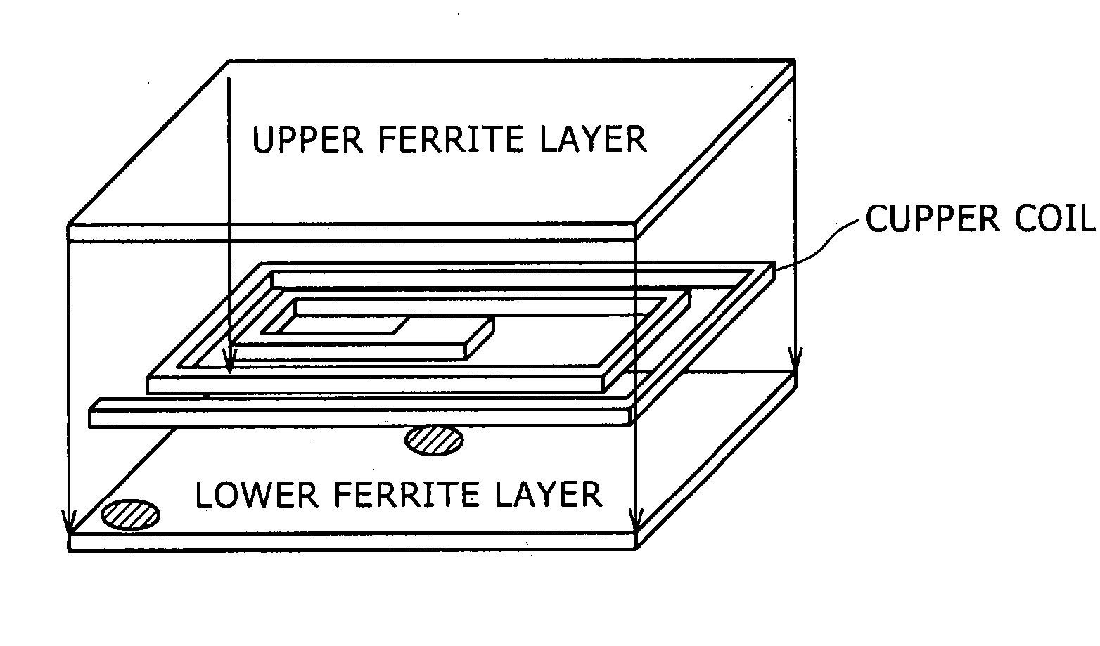
[0065] The inductor element according to an embodiment of the present invention should have both the substrate of magnetic material and the layer of magnetic material formed from a high-permeability material, so that the coil is embedded in the high-permeability material. This structure permits the inductor element to exhibit a high inductance.

[0066] Both the substrate of magnetic material and the layer of magnetic material should preferably be formed from ferrite. Being formed from ferrite by aerosol deposition, the layer of magnetic material, which is thicker than 50 μm, has a compact structure, so that the inductor element is thin and small and yet has a high inductance.

[0067] The coil should preferably be a planar coil thicker than 50 μm, so that it has a large sectional area that permits a large allowable current (maximum current) to flow through the inductor element.

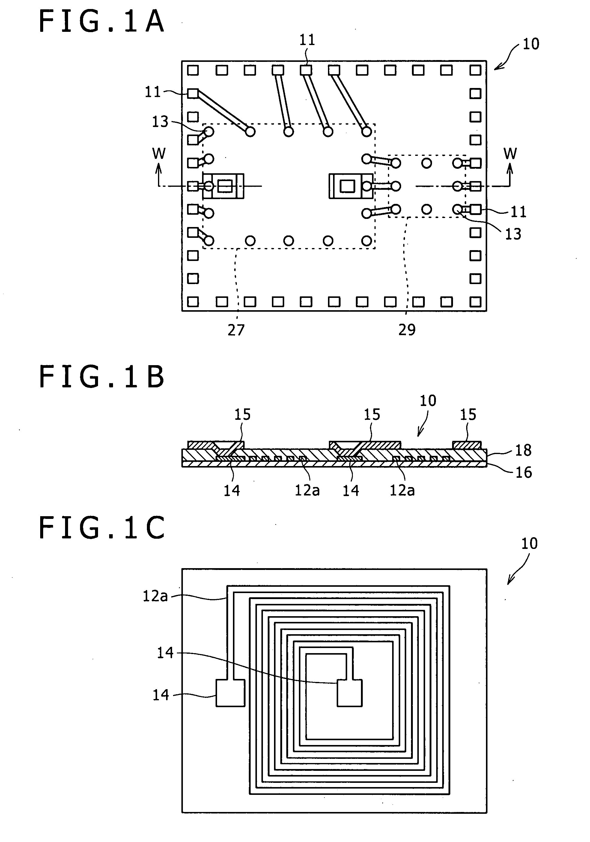
[0068] The inductor element should have terminals connected to the ends of the coil on the outside of the lay...


PUM

PropertyMeasurementUnit
thicknessaaaaaaaaaa
thicknessaaaaaaaaaa
thicknessaaaaaaaaaa

Abstract

An inductor element includes a substrate of magnetic material, a coil, and a layer of magnetic material. The coil of conductive material is formed on the substrate. The layer of magnetic material is so formed by aerosol deposition as to enclose the coil on the substrate of magnetic material.

Description

CROSS REFERENCES TO RELATED APPLICATIONS [0001] The present invention contains subject matter related to Japanese Patent Application JP 2006-073837 filed with the Japanese Patent Office on Mar. 17, 2006, the entire contents of which being incorporated herein by reference. BACKGROUND OF THE INVENTION [0002] 1. Field of the Invention [0003] The present invention relates to an electronic component and, more particularly, to a small-sized inductor element having a large inductance and a high quality factor and a method for production thereof, and also to a semiconductor module with the inductor element. [0004] 2. Description of the Related Art [0005] Inductors fall under several categories according to their structure, such as wire-wound coil, laminated coil, and thin-film coil. The laminated coil is composed of layers of ferrite or ceramic material placed one over another, each layer having a conductor pattern printed thereon, such that all the printed conductor patterns are connected ...

Claims


Application Information

Patent Timeline
Patent Type & Authority Applications(United States)
IPC IPC(8): H01F5/00
CPCH01F1/344Y10T29/4902H01F41/046H01F2017/0066H01L21/563H01L23/14H01L23/3128H01L23/645H01L25/0655H01L2224/48091H01L2224/73203H01L2924/01046H01L2924/01078H01L2924/01079H01L2924/09701H01L2924/15311H01L2924/19041H01L2924/19105H01L2924/19106H01L2924/30107H01L2924/3025H01F17/0006H01L2924/01047H01L2924/01015H01L2924/19107H01L2224/16225H01L24/48H01L2224/45147H01L2924/00014H01L2924/00H01L24/45H01L2924/181H01L2224/32225H01L2224/73204H01L2924/00011H01L2924/15192H01L2224/16265H01L2224/45099H01L2924/00012H01L2924/01005H01L27/02H01F17/00
Inventor OYA, YOICHIYANAGAWA, SHUSAKUOKA, SHUICHI
Owner SONY CORP
Why Eureka
Try Eureka