Semiconductor device package and method of production and semiconductor device of same

a technology of semiconductor devices and semiconductor chips, applied in the direction of basic electric elements, thin/thick film capacitors, printed circuit non-printed electric components association, etc., can solve the problems of easy unstable power supply to semiconductor chips b>102/b>, and achieve the effect of reducing the inductance shortening the distance of the conductor circuit, and reducing the connection location

Inactive Publication Date: 2005-07-05
SHINKO ELECTRIC IND CO LTD
View PDF6 Cites 49 Cited by
  • Summary
  • Abstract
  • Description
  • Claims
  • Application Information

AI Technical Summary

Benefits of technology

[0024]Therefore, since the electrode terminals of the semiconductor chip and the electrode terminals of the capacitor are connected through the connection pads or directly, it is possible to shorten the distance of the conductor circuit between terminals as much as possible and reduce the connection locations and possible to reduce the inductance of the conductor circuit electrically connecting the electrode terminals of the semiconductor chip and electrode terminals of the capacitor.

Problems solved by technology

Due to this, it was learned that the power supplied to the semiconductor chip 102 easily became unstable.

Method used


Image

  • Semiconductor device package and method of production and semiconductor device of same
  • Semiconductor device package and method of production and semiconductor device of same
  • Semiconductor device package and method of production and semiconductor device of same

Examples


Embodiment Construction

[0036]Preferred embodiments of the present invention will be described in detail below while referring to the attached figures.

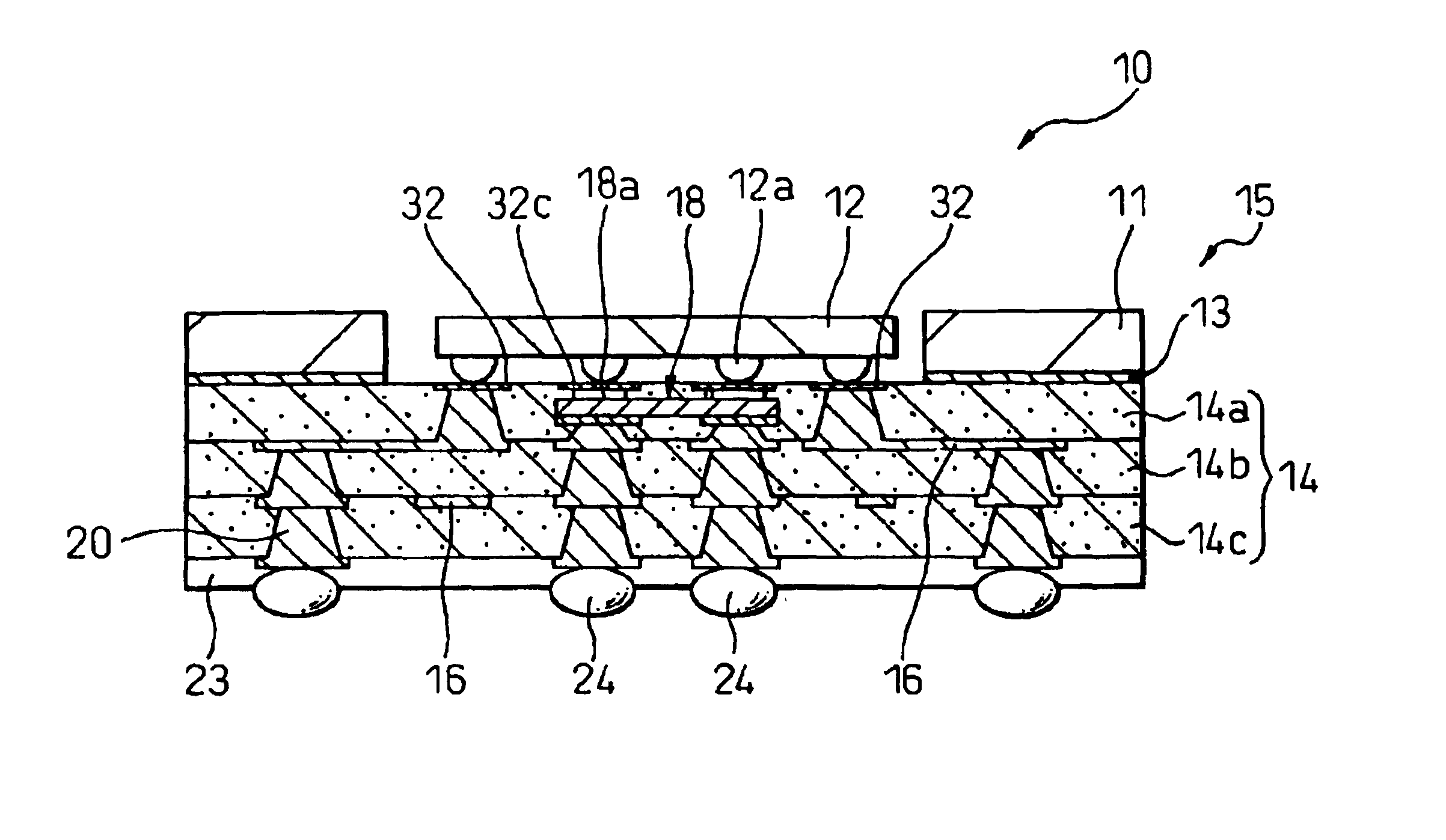
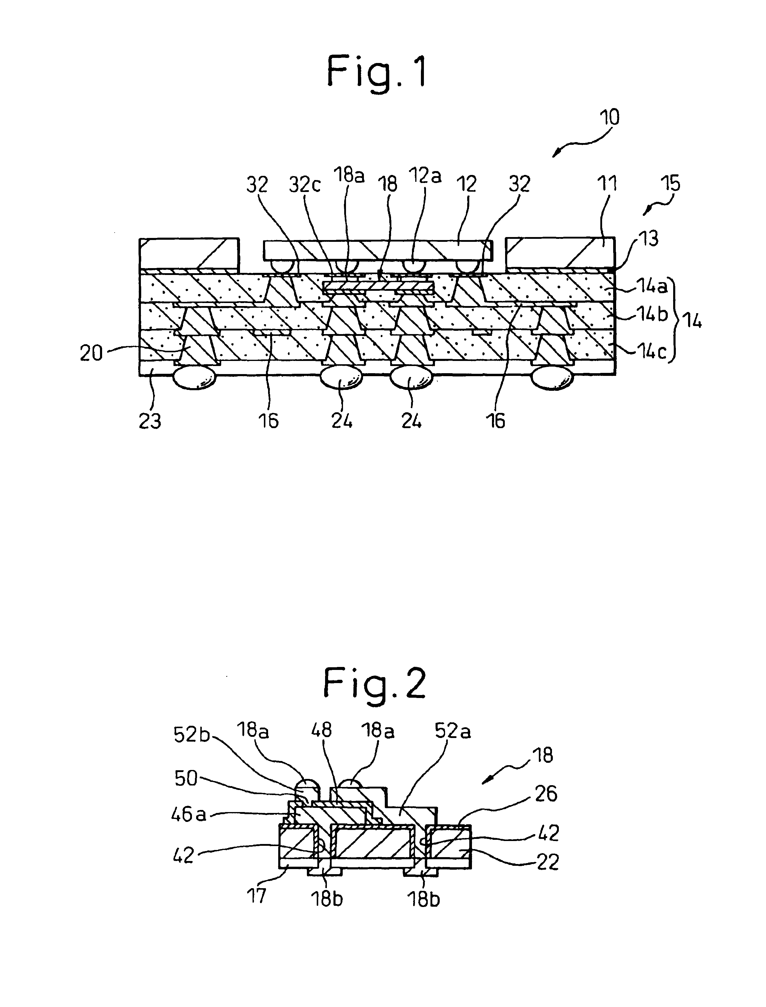
[0037]A semiconductor device according to the present invention is shown in FIG. 1. The semiconductor device 10 shown in FIG. 1 is comprised of a semiconductor device package 14 (hereinafter sometimes simply referred to as a “package”) provided inside it with a capacitor 18, a frame-shaped metal plate 11 serving as a reinforcing member bonded to one surface of the same by a thin resin layer 13, and a semiconductor chip 12 mounted by flip-chip bonding to a semiconductor chip mounting surface formed in a frame-shaped opening of the metal plate 11.

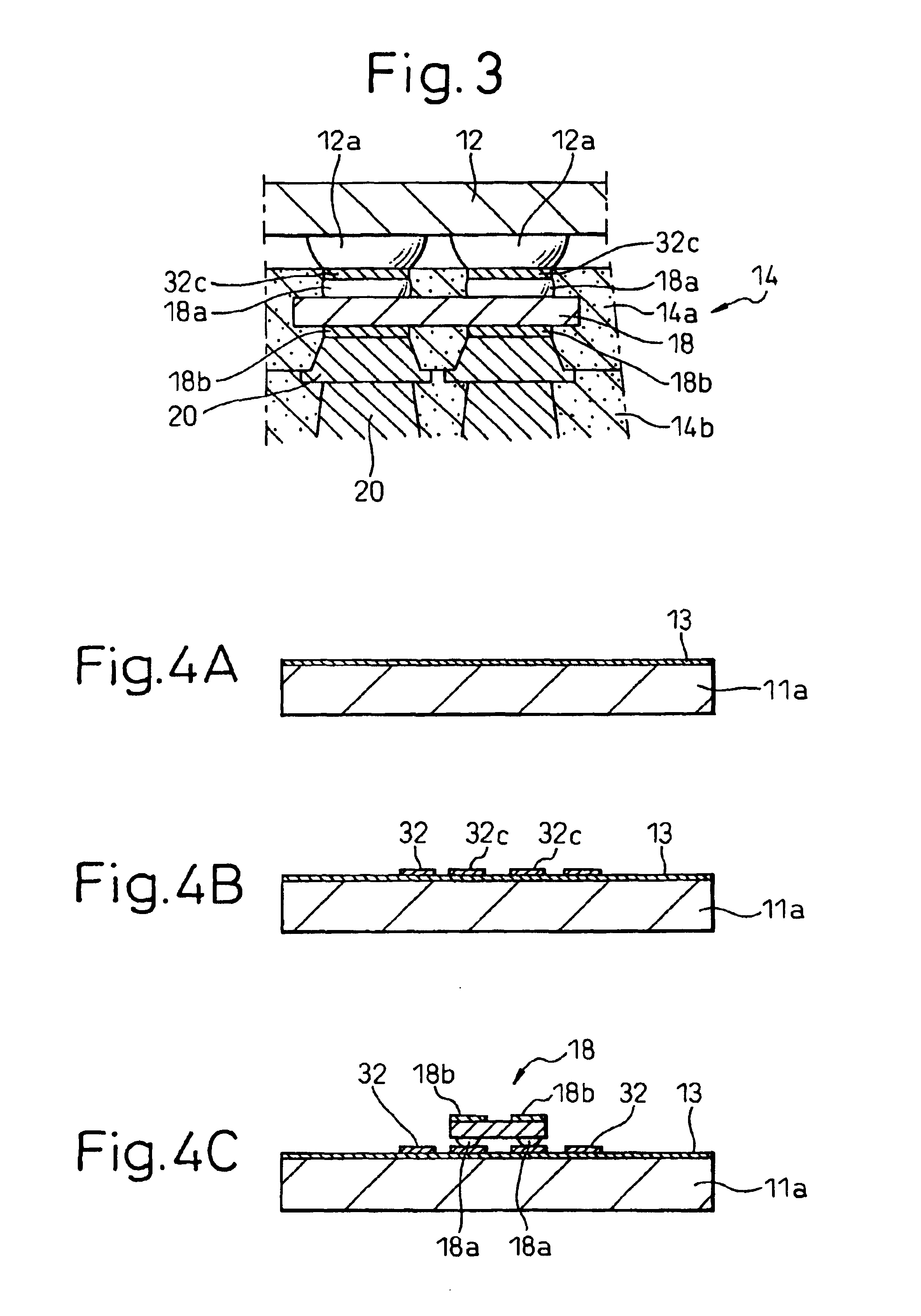
[0038]The package 14 is a multilayer circuit board comprised of a stack of resin layers 14a, 14b, and 14c serving as insulating layers formed with conductor patterns 16, 16 . . . The conductor patterns 16, 16 . . . formed on the layers are electrically connected by vias 20, 20 . . . formed through the layers.

[0039]The...


PUM


Abstract

A semiconductor device including a semiconductor device package providing a capacitor in its circuit board and a semiconductor chip mounted on that package, wherein the capacitor is provided directly under a semiconductor chip mounting surface of the circuit board on which the semiconductor chip is to be mounted and the conductor circuit electrically connecting the semiconductor chip and capacitor is made the shortest distance by having the external connection terminals of the capacitor directly connected to the other surface of the connection pads exposed at one surface at the semiconductor chip mounting surface of the circuit board and to which the electrode terminals of the semiconductor chip are to be directly connected.

Description

BACKGROUND OF THE INVENTION[0001]1. Field of the Invention[0002]The present invention relates to a semiconductor device package and a method of production and semiconductor device of the same, more particularly relates to a semiconductor device package providing a capacitor in a circuit board on which a semiconductor chip is mounted and a method of production and semiconductor device of the same.[0003]2. Description of the Related Art[0004]In recent years, semiconductor devices have been mounting higher operating frequency semiconductor chips. Along with this, it is becoming necessary to stabilize the power supplied to the semiconductor chips. Therefore, chip capacitors or other capacitors are being provided in the semiconductor device packages mounting the semiconductor chips.[0005]One of the inventors of this application previously proposed the semiconductor device shown in FIG. 10 in the specification of Japanese Patent Application No. 2000-276514 as a semiconductor device using ...

Claims


Application Information

Patent Timeline
Patent Type & Authority Patents(United States)
IPC IPC(8): H01L23/498H01L23/48H05K1/18H01L23/12H05K3/46
CPCH01L23/49822H05K1/185H05K1/187H01G4/33H01L2224/16H01L2924/01078H01L2924/15311H01L2224/16235H01L2224/16237H01L2224/05001H01L2224/05027H01L2224/05569H01L2224/05024H01L2224/05008H01L2224/05548H01L2224/05571H01L24/05H01L23/12
Inventor IIJIMA, TAKAHIROROKUGAWA, AKIO
Owner SHINKO ELECTRIC IND CO LTD
Why Eureka
Try Eureka