Enhancement mode III-nitride FET

a technology of nitride and enhanced mode, which is applied in the direction of semiconductor/solid-state device manufacturing, semiconductor devices, electrical apparatus, etc., can solve the problems of limited applicability to power management, limited thickness of strained algan/gan system, and limited thickness of low resistive loss and high current densities. , to achieve the effect of low leakage, low resistance and high breakdown field

Active Publication Date: 2008-06-03
INFINEON TECH AMERICAS CORP
View PDF24 Cites 89 Cited by
  • Summary
  • Abstract
  • Description
  • Claims
  • Application Information

AI Technical Summary

Benefits of technology

[0028]In another advantage of the present invention, a pair of nominally off bi-directional switches may be realized in a single semiconductor structure to form a bi-directional half bridge circuit with a common drain, for example. Bi-directional half bridge arrangement is useful in a number of applications including motor drive systems, power converters and other well known power control applications. For example, a number of nominally off bidirectional switches may be realized in a single device to create a three-phase bridge circuit, a full-bridge circuit or a half-bridge circuit. In addition, the device according to the present invention may be incorporated into a Schottky bridge.
[0029]According to one embodiment of the present invention, a nominally off FET device with a gate, source and drain area are defined using a two layer AlGaN / GaN material to produce a III-nitride HEMT device. The source and drain regions may be formed according to known methods including ion implantation, etching to remove the barrier region over the source and drain regions and application of a low resistance ohmic contact formation process.
[0030]The device is also characterized by low leakage in the gate contact and a high breakdown field from the barrier layer. As a result, the device provides a larger dielectric constant compared to conventional insulators such as SiO2 and SiN. The high critical fields of the GaN material allow thin layers to withstand large voltages without dielectric breakdown. The dielectric constant of GaN materials is approximately 10, which is a factor of 2.5 times better than SiO2.

Problems solved by technology

The nominally on nature of the HEMT devices previously fabricated have limited their applicability to power management.
The limitations of nominally on power devices is observed in the need to have a control circuit be powered and operational, before power can be safely controlled by a III-nitride HEMT device.
A drawback of III-nitride HEMT devices that permit high current densities with low resistive losses is the limited thickness that can be achieved in the strained AlGaN / GaN system.
The difference in the lattice structures of these types of materials produces a strain that can result in dislocation of films grown to produce the different layers.
This results in high levels of leakage through a barrier layer, for example.
However, the problem of limited thickness is not addressed by these designs.
While additional insulator layers can permit thicker strained AlGaN / GaN systems to be constructed, the confinement layer produced by the additional insulator results in lower current carrying capacity due to the scattering effect produced on electrons at the GaN / insulator interface.
Also, the additional interface between the AlGaN layer and the insulator results in the production of interface trap states that slow the response of the device.
These devices, however, typically have lower current carrying capacity due to scattering at the GaN / insulator interface.
However, forming gallium nitride materials on silicon substrates to produce semiconductor devices presents challenges that arise from differences in the lattice constant, thermal expansion and bandgap between silicon and gallium nitride.
The problems attendant with the lattice mismatch between GaN and traditional substrate materials are also prevalent in material layer structures involving GaN and GaN alloys.
Presently, bi-directional devices are somewhat complex and typically composed of a number of discrete IC devices.

Method used


Image

  • Enhancement mode III-nitride FET
  • Enhancement mode III-nitride FET
  • Enhancement mode III-nitride FET

Examples


Embodiment Construction

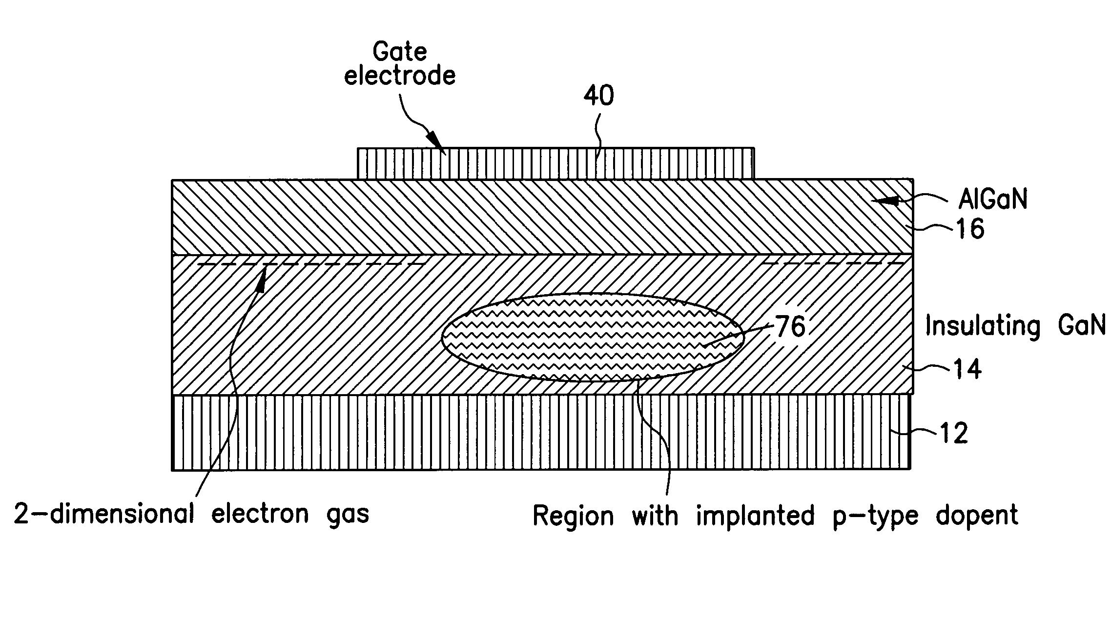
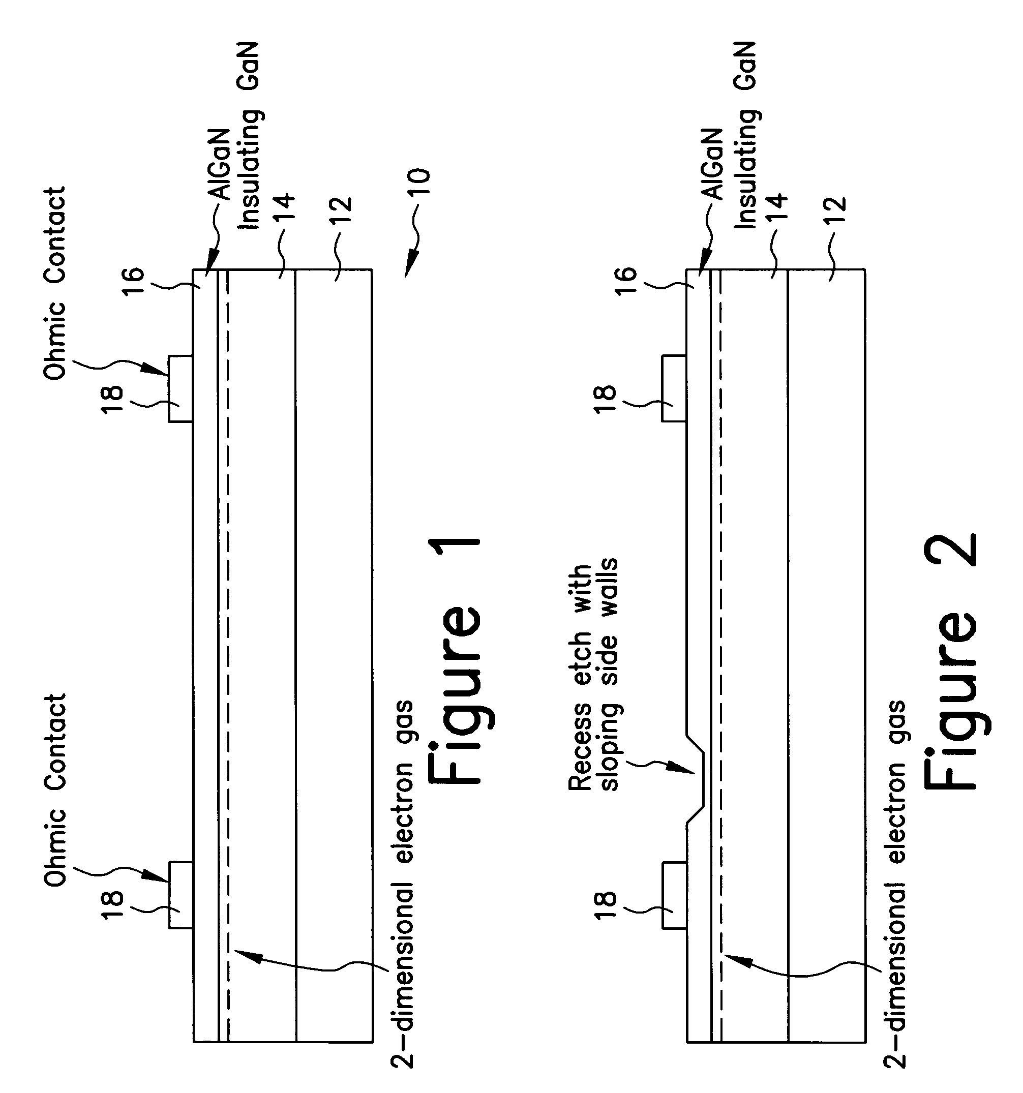
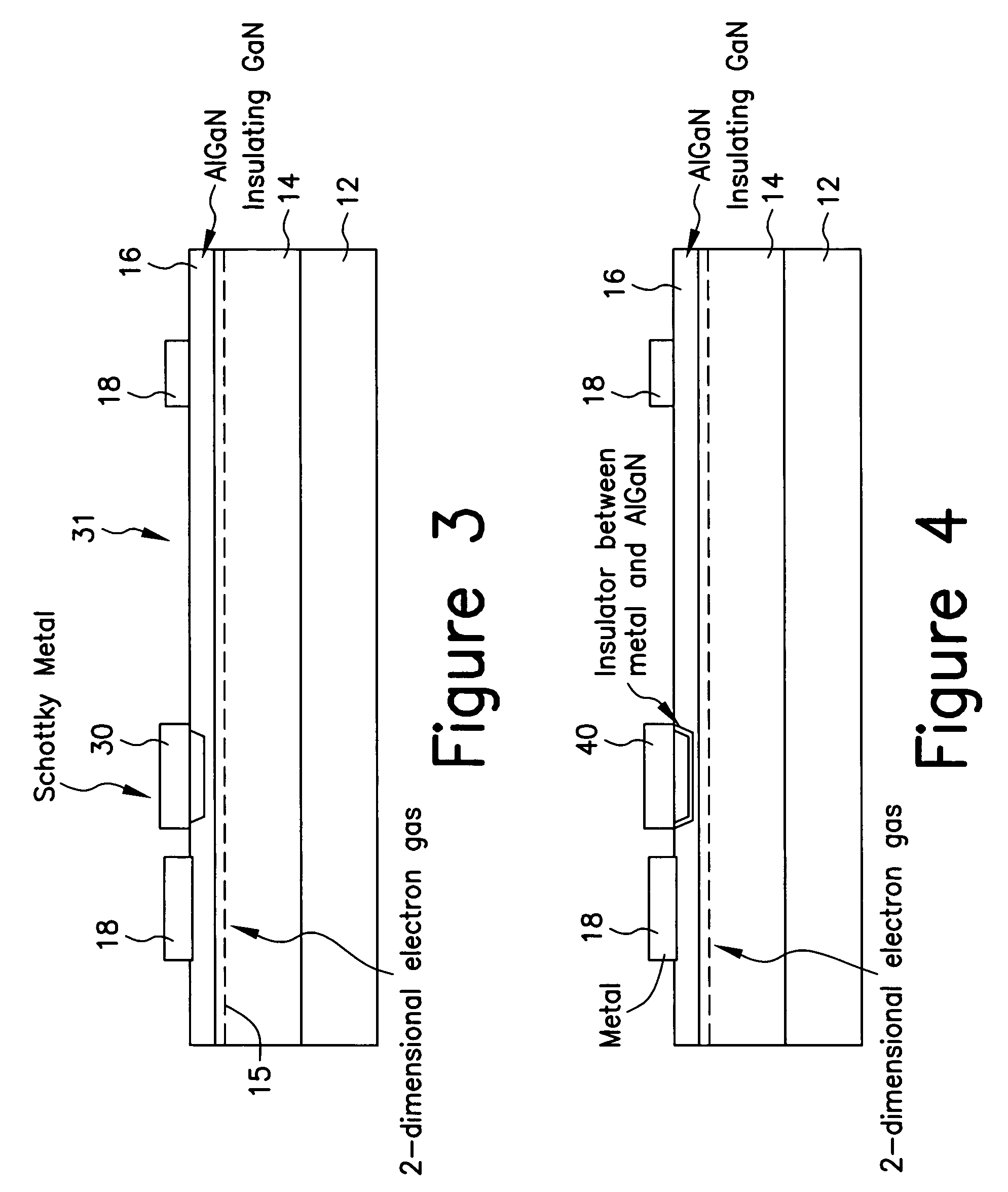
[0039]In the construction of GaN material devices, a number of factors come into play to impact the functionality and capability of the devices. A large lattice mismatch in III-nitride materials and the strong piezoelectric and polarization effects in these materials significantly impact the electrical properties of III-nitride heterojunction devices. Nearly all reported GaN-based HEMTs to date use strained GaN—AlGaN junctions with alloy compositions that are designed to relieve the strain to avoid dislocations that may be responsible for long term instabilities in the devices. Various devices and systems for building heterojunction devices have been proposed to control the lattice mismatch and the strain of the GaN—AlGaN junctions. These devices are particularly designed to take advantage of piezoelectric and spontaneous polarization effects and to minimize long term instabilities.

[0040]GaN / AlGaN HEMT devices typically have three terminals including a gate, a drain and a source ter...


PUM


Abstract

A III-nitride switch includes a recessed gate contact to produce a nominally off, or an enhancement mode, device. By providing a recessed gate contact, a conduction channel formed at the interface of two III-nitride materials is interrupted when the gate electrode is inactive to prevent current flow in the device. The gate electrode can be a schottky contact or an insulated metal contact. Two gate electrodes can be provided to form a bi-directional switch with nominally off characteristics. The recesses formed with the gate electrode can have sloped sides. The gate electrodes can be formed in a number of geometries in conjunction with current carrying electrodes of the device.

Description

CROSS-REFERNCE TO RELATED APPLICATION[0001]The present application is based on and claims benefit of U.S. Provisional Application No. 60 / 538,795, filed Jan. 23, 2004, entitled Enhancement Mode FET Based on Etched Gate, to which a claim of priority is hereby made and the disclosure of which is incorporated by reference.BACKGROUND OF THE INVENTION[0002]1. Field of the Invention[0003]The present invention relates generally to a class of field effect transistors based on III-nitride materials, and relates more particularly to an enhancement mode.[0004]2. Description of Related Art[0005]III-nitride semiconductors are presently known that exhibit a large dielectric breakdown field of greater than 2.2 MV / cm. III-nitride heterojunction structures are also capable of carrying extremely high currents, which makes devices fabricated in the III-nitride material system excellent for power applications.[0006]Development of devices based on III-nitride materials has generally been aimed at high po...

Claims


Application Information

Patent Timeline
Patent Type & Authority Patents(United States)
IPC IPC(8): H01L29/739H01L31/0328H01L31/0336H01L31/072H01L31/109H01L21/335H01L29/20H01L29/778
CPCH01L29/0623H01L29/32H01L29/66431H01L29/4236H01L29/66462H01L29/7787H01L29/42316H01L29/1066H01L29/2003H01L29/772
Inventor BEACH, ROBERT
Owner INFINEON TECH AMERICAS CORP
Why Eureka
Try Eureka