Deposition of hafnium oxide and/or zirconium oxide and fabrication of passivated electronic structures

a technology of zirconium oxide and hafnium oxide, which is applied in the field of electromechanical devices, can solve the problems of difficult manufacture and thickness control, increased manufacturing costs, and reduced thickness, and achieves the effect of reducing the conditions necessary, and reducing the amount of emitted

Inactive Publication Date: 2006-01-03
GLOBALFOUNDRIES INC
View PDF13 Cites 114 Cited by
  • Summary
  • Abstract
  • Description
  • Claims
  • Application Information

AI Technical Summary

Benefits of technology

[0008]The applicants of the present invention have discovered that the method of depositing the high-k oxide including precursor selection, precursor delivery, growth conditions and Si substrate modification is critical in achieving a film which does not require a post deposition anneal, and is stable to reducing conditions necessary to passivate the underlying silicon. The applicants have also discovered that by careful selection of the CVD (chemical vapor deposition) precursor with optimal decomposition pathways, careful selection of the precursor delivery method, and careful selection of growth conditions, one can grow a smooth, crystalline, metal oxide film with suitable properties for incorporation into an electronic device without the need of a post deposition anneal. It has also been discovered that the resultant film is stable under reducing conditions necessary to passivate the underlying silicon. The applicants have further discovered that by careful selection of passivating conditions, one can fabricate a device with superior electrical properties with minimal flat band voltage shift, an appropriate threshold voltage, low inversion thickness, and enhanced mobility.

Problems solved by technology

In the quest for improved performance, electronic circuits are becoming denser and devices smaller.
However, as the thickness of SiO2 approaches 15 Å, substantial problems appear, including large leakage currents through the gate dielectric, concerns about the long-term dielectric reliability, and difficulty of manufacture and thickness control.
Similar problems are encountered in scaling capacitors in memory devices.
Unfortunately, other problems have arisen from utilizing high-k dielectrics in CMOS devices including difficulty in passivating the underlying silicon, the introduction of unwanted charges in the gate stack which produce large flat band voltage shifts, large threshold voltage shifts, significant charge trapping, and low mobility devices.
However, control of growth rate necessary to achieve thin films (<100 Å) is difficult with conventional bubbler technology, due to fluctuations in precursor flux caused by variations in bubbler temperature, first run effects (bubbler held at elevated temperature in static conditions over time will have a higher volatilized precursor concentration, than a bubbler which is dynamically purged), and precursor volatility changes due to sintering of solids and / or precursor decomposition.
Elevated temperatures and thermal cycling of a precursor in a conventional bubbler may contribute to premature degradation by ligand rearrangement, cluster formation, or oxidation of liquid and solid precursors over time.
An additional problem with high-k dielectrics is that they tend to be oxygen deficient.
The interfacial SiO2 layer reduces the effectiveness of the high-k dielectrics, since SiO2 has a lower dielectric constant and thus reduces the effective capacitance of the film.
An additional problem associated with post deposition annealing of the above-mentioned high-k dielectrics is that during post deposition annealing, crystallization and grain growth may occur.
As a result, the surface of the annealed film may roughen.
Surface roughness causes non-uniform electrical fields in the channel region adjacent the dielectric film.
Such films are not suitable for the gate dielectrics of MOSFET devices.
An additional problem associated with high-k dielectrics is their sensitivity to reducing conditions, specifically to forming gas anneals.
However, subjection of a metal oxide to a reducing environment commonly results in diminished electronic properties due to reduction of the metal oxide.
Commonly, a dramatic increase in leakage current is observed.
Strategies such as recovery anneal in oxygen to reoxidize the metal oxide has the disadvantage of negating the effect of the forming gas anneal on the underlying silicon.
Encapsulation techniques and barrier layers to slow the diffusion of hydrogen to the metal oxide require additional processing steps and are not completely effective.

Method used


Image

  • Deposition of hafnium oxide and/or zirconium oxide and fabrication of passivated electronic structures
  • Deposition of hafnium oxide and/or zirconium oxide and fabrication of passivated electronic structures
  • Deposition of hafnium oxide and/or zirconium oxide and fabrication of passivated electronic structures

Examples


example 1

Chemical Vapor Deposition of Hafnium Oxide

[0059]The hafnium oxide films were deposited in a quartz horizontal hot wall CVD reactor equipped with a 1×3×8″ quartz flow cell. An ATMI (Advanced Technology and Materials, Inc. Danbury, CT) LDS 300B liquid delivery system and vaporizer was used to introduce precursors into the reactor. The hafnium alkoxide source mixture was comprised of 40 grams of hafnium tert-butoxide Hf(t-OC4H9)4 and 1 liter of octane. A thin layer (xNy layer was deposited on the silicon wafer prior to growth of hafnium oxide. The hafnium alkoxide source mixture was flowed at 0.5–0.01 ml / min, preferably 0.05 ml / min. The vaporizer temperature was 120–180° C., preferably 120° C. Anhydrous nitrogen was introduced into the vaporizer at 20–2000 sccm, preferably 200 sccm as a carrier gas for the volatilized hafnium isopropoxide. A reactant gas selected from the group including, oxygen, N2O, NO, H2O, ozone, preferably, oxygen was introduced through a separate inlet as the rea...

example 2

Chemical Vapor Deposition of Hafnium Oxide

[0062]The hafnium oxide films were deposited in a single wafer, lamp heated susceptor type CVD reactor equipped with a 300 mm showerhead as supplied by TEL. A liquid delivery system and vaporizer was used to introduce precursors into the reactor. The hafnium alkoxide source mixture was comprised of 40 grams of hafnium tert-butoxide and 1 liter of octane. A thin layer (2) oxide (UTO) or rapid thermal thin oxide containing nitrogen (RTNO) was deposited on the silicon wafer prior to growth of hafnium oxide. The hafnium alkoxide source mixture was flowed at between 1 and 400 mg / min, preferably 80. The vaporizer temperature was 30–300° C., preferably 50° C. Anhydrous nitrogen was introduced into the vaporizer at 10–2000 sccm, preferably 40 sccm as a carrier gas for the volatilized hafnium tert-butoxide. Oxygen was introduced through a separate inlet as the reactant gas. The system pressure was 1 mT to 100 Torr during growth, preferably 1.5 Torr. ...

example 3

Chemical Vapor Deposition of Hafnium Oxide

[0063]In this embodiment, the liquid is not vaporized and is diverted from the CVD reactor. The hafnium alkoxide is dissolved, emulsified or suspended in a liquid which vaporizes at a higher temperature. The hafnium alkoxide and the liquid is introduced into a vaporizer where the hafnium alkoxide is vaporized. The liquid is not vaporized, but instead is diverted from the reactor in liquid form.

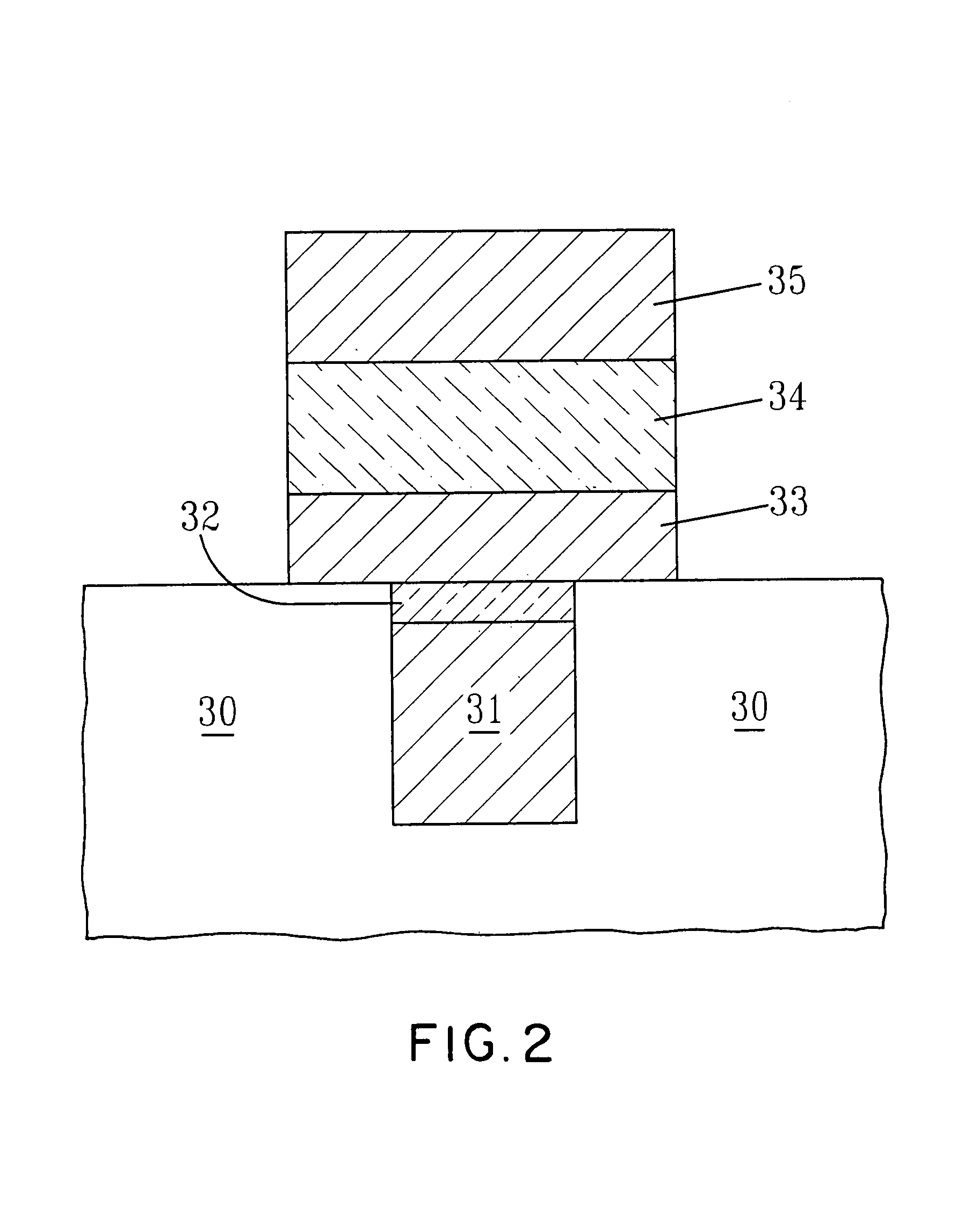
[0064]One possible apparatus configuration is shown in FIG. 5. As shown in FIG. 5, the hafnium alkoxide and liquid would flow from ampoule 100 to vaporizer 102. The hafnium alkoxide is volatilized in the vaporizer, but the liquid would not. The vaporized hafnium alkoxide is then transported to reactor 106, and the nonvaporized inert liquid is drained out of the vaporizer and collected in trap 04. The vaporizer temperature is set at less than the boiling point of the liquid. Inlet 101 and outlet 103 are also shown, together with arrows which depict the ...


PUM

PropertyMeasurementUnit
temperatureaaaaaaaaaa

Abstract

A method of fabricating hafnium oxide and/or zirconium oxide films is provided. The methods include providing a mixture of Hf and/or Zr alkoxide dissolved, emulsified or suspended in a liquid; vaporizing at least the alkoxide and depositing the vaporized component at a temperature of greater than 400° C. The resultant film is dense, microcrystalline and is capable of self-passivation when treated in a hydrogen plasma or forming gas anneal.

Description

FIELD OF THE INVENTION[0001]The present invention relates to electronic devices, and more particular to a method of fabricating passivated electronic devices that contain hafnium oxide and / or zirconium oxide deposited by chemical vapor deposition.BACKGROUND OF THE INVENTION[0002]In the quest for improved performance, electronic circuits are becoming denser and devices smaller. For example, the most common gate dielectric in metal-oxide semiconductor field-effect transistors (MOSFETs) has been SiO2. However, as the thickness of SiO2 approaches 15 Å, substantial problems appear, including large leakage currents through the gate dielectric, concerns about the long-term dielectric reliability, and difficulty of manufacture and thickness control. A solution to the problem is to use thick films of materials, such as hafnium oxide (HfO2) and / or zirconium oxide (ZrO2) which have a dielectric constant larger than SiO2. Thus, the physical thickness of the gate dielectric can be large, while t...

Claims


Application Information

Patent Timeline
Patent Type & Authority Patents(United States)
IPC IPC(8): H01L21/31C23C16/40C23C16/56H01L21/28H01L21/316H01L21/336H01L21/8238H01L27/08H01L29/49H01L29/51
CPCC23C16/405C23C16/56H01L21/28185H01L21/28194H01L21/28202H01L21/31604H01L21/823857H01L27/0805H01L29/513H01L29/66545H01L2924/0002H01L29/495H01L29/4966H01L29/517H01L29/518H01L2924/00H01L21/02205H01L21/02189H01L21/02271H01L21/02181
Inventor CABRAL, JR., CYRILCALLEGARI, ALESSANDRO C.GRIBELYUK, MICHAEL A.JAMISON, PAUL C.LACEY, DIANNE L.MCFEELY, FENTON R.NARAYANAN, VIJAYNEUMAYER, DEBORAH A.RANADE, PUSHKARZAFAR, SUFI
Owner GLOBALFOUNDRIES INC
Why Eureka
Try Eureka