Method of forming a static random access memory with a buried local interconnect

a static random access memory and local interconnect technology, applied in the field of static random access memory with buried local interconnect, method of forming structure, can solve problems such as difficult process implementation, and achieve the effect of reducing the contact space and the number of contacts needed

Active Publication Date: 2006-01-26
TAIWAN SEMICON MFG CO LTD
View PDF18 Cites 97 Cited by
  • Summary
  • Abstract
  • Description
  • Claims
  • Application Information

AI Technical Summary

Benefits of technology

[0011] According to the preferred embodiment, the SRAM cell uses a minimum number of contact, metal and via layers. This LI also benefits the cell contact/metal routing rules and provides the smallest cell structure and minimum metal layers. The butted contact (e.g., rectangular contact, shared contact, longer contact) is a very popular technology that can reduce the contact space and number of contacts needed. But thi...

Problems solved by technology

But this process is difficult to implement (e.g., in the lithography and etch module) due to the inhere...

Method used


Image

  • Method of forming a static random access memory with a buried local interconnect
  • Method of forming a static random access memory with a buried local interconnect
  • Method of forming a static random access memory with a buried local interconnect

Examples


Embodiment Construction

[0020] The making and using of the presently preferred embodiments are discussed in detail below. It should be appreciated, however, that the present invention provides many applicable inventive concepts that can be embodied in a wide variety of specific contexts. The specific embodiments discussed are merely illustrative of specific ways to make and use the invention, and do not limit the scope of the invention.

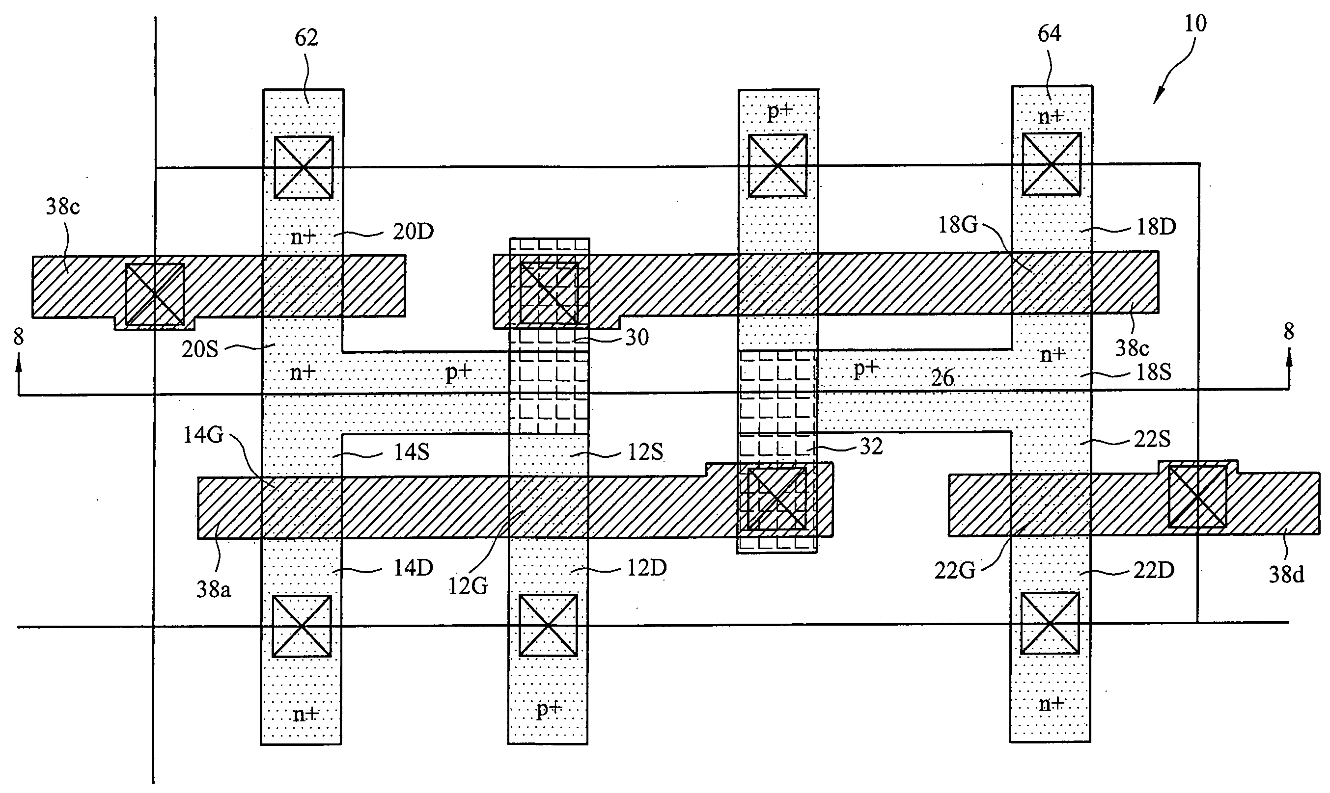
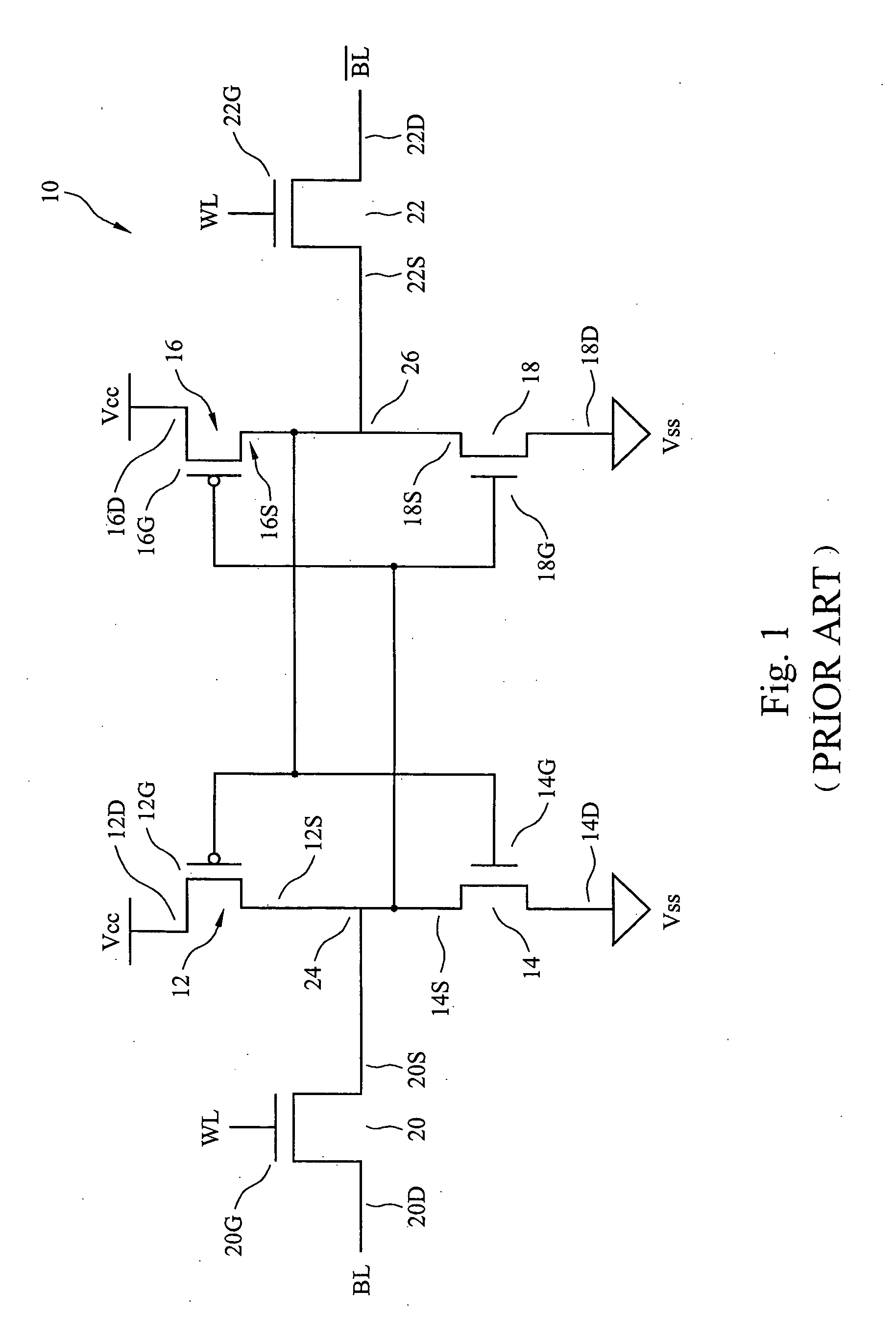
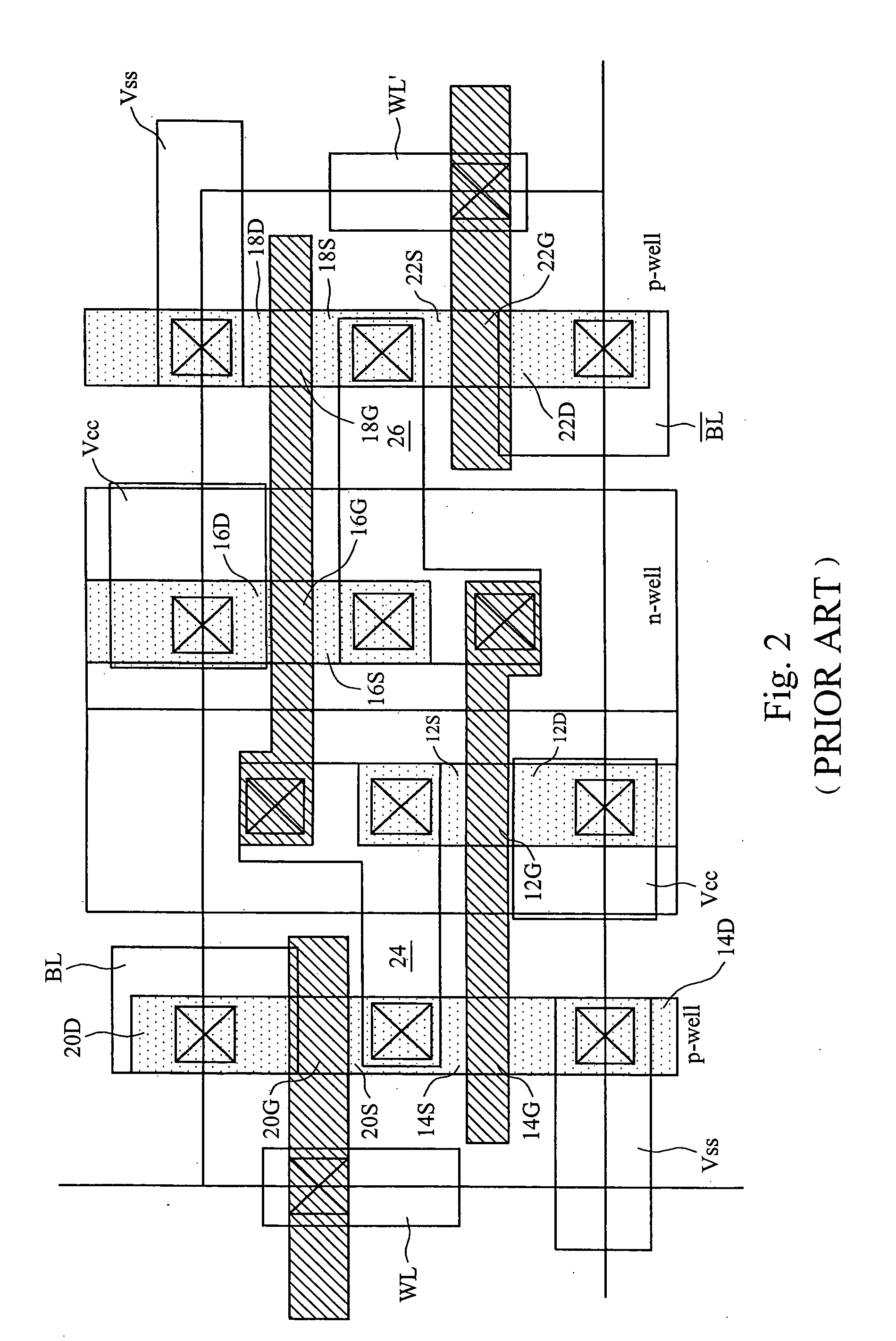
[0021]FIG. 4a shows the layout of a first embodiment SRAM cell of the present invention. The schematic diagram of the device is shown in FIG. 1 and, therefore, the various regions have been labeled to correspond with the labels used in FIG. 1.

[0022] As discussed above, the SRAM 10 of FIG. 4a includes six transistors. In particular, p-channel pull-up transistor 12 includes drain 12D coupled to a high voltage supply node Vcc (e.g., held at a voltage such as 1.5V, 2.4V or 3.3V) and a source 12S coupled to a first storage node 24. In another embodiment, the high voltage supply...


PUM


Abstract

An SRAM cell includes six transistors. The storage nodes are implemented using local interconnects. A first level of metal overlies the interconnects but is electrically isolated therefrom. Contact plugs are formed to couple the cell to the first level of metal. The contact plugs are preferably formed in a different process step than the interconnects.

Description

[0001] This is a continuation-in-part of U.S. application Ser. No. 10 / 898,456, filed on Jul. 23, 2004, and incorporated herein by reference.TECHNICAL FIELD [0002] The present invention relates generally to semiconductor structures and methods and more particularly to a method of forming a structure, such as static random access memory, with a buried local interconnect. BACKGROUND [0003] Electronic devices, including mobile and portable devices such as cell phones, personal digital assistants (PDA), and digital cameras, use static random access memory (SRAM) chips with a high storage density. In deep submicron technology, a large number of SRAM cells are used in products such as microprocessors, communications chips and system on a chip (SOC) applications. One ongoing goal is to reduce the size of each cell in order to lower overall costs. [0004]FIG. 1 shows a schematic diagram of a conventional six-transistor (6T) SRAM cell 10. In this cell, a first inverter includes p-channel trans...

Claims


Application Information

Patent Timeline
IPC IPC(8): H01L21/8234
CPCH01L27/1104H01L27/11H10B10/00H10B10/12
Inventor LIAW, JHON-JHY
Owner TAIWAN SEMICON MFG CO LTD
Why Eureka
Try Eureka