Highly efficient gallium nitride based light emitting diodes via surface roughening

a gallium nitride and light-emitting diode technology, applied in the field of high-efficiency gallium nitride-based light-emitting diodes via surface roughening, can solve the problems of little room for improvement of these values, difficult and costly for this kind of led structure to be produced, and inability to readily achieve the increase of internal quantum efficiency

Active Publication Date: 2010-02-04
RGT UNIV OF CALIFORNIA
View PDF29 Cites 59 Cited by
  • Summary
  • Abstract
  • Description
  • Claims
  • Application Information

AI Technical Summary

Benefits of technology

[0022]The present invention describes a gallium nitride (GaN) based light emitting diode (LED), wherein light is extracted through a nitrogen face (N-face) of the LED and a surface of the N-face is roughened into one or more hexagonal shaped cones. The roughened surface reduces light reflections occurring repeatedly inside the LED, and thus extracts more light out of the LED.

Problems solved by technology

Increasing the internal quantum efficiency cannot readily be done.
There is little room for improvement of these values.
However, surface roughened LEDs have been mentioned only in the context of the gallium phosphide (GaP) family of materials, because GaN is very durable material and an ordinary wet etching method does not have much effect.
Thus, although the idea of roughening the semiconductor surface for the sake of scattering light was first considered in the 1970's, it has been believed to be difficult and costly for this kind of LED structure to be produced.
Although producing a roughened surface requires a certain GaN layer thickness [6], growing thick p-GaN is not desirable due to the relatively high resistivity of p-GaN, which demands a semi-transparency contact on the p-GaN surface if the light is extracted through the p-GaN, and some treatments such as dry etching [7] for roughening surfaces might cause electrical deterioration.
Growing a p-side down structure by metalorganic chemical vapor deposition (MOCVD) is also undesirable, because of the magnesium (Mg) memory effect [8], which deteriorates the active layer.
However, there was no reference to the effect of this technique on surface morphology or extraction efficiency.
The use of dry etching to make a textured surface is possible, but requires extra processing, such as photolithography, and it is impossible to make a fine cone-like surface on the GaN.

Method used


Image

  • Highly efficient gallium nitride based light emitting diodes via surface roughening
  • Highly efficient gallium nitride based light emitting diodes via surface roughening
  • Highly efficient gallium nitride based light emitting diodes via surface roughening

Examples


Embodiment Construction

[0036]In the following description of the preferred embodiment, reference is made to the accompanying drawings which form a part hereof, and in which is shown by way of illustration a specific embodiment in which the invention may be practiced. It is to be understood that other embodiments may be utilized and structural changes may be made without departing from the scope of the present invention.

[0037]Overview

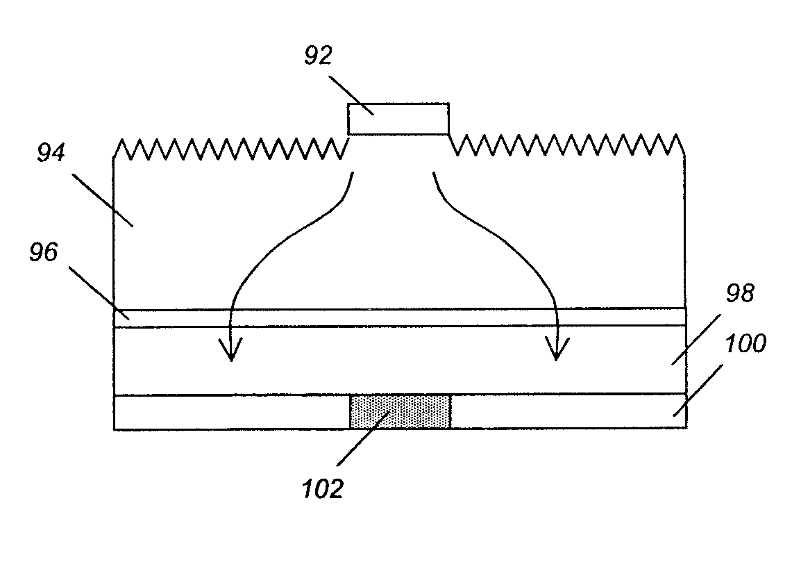
[0038]The present invention provides a means of increasing the extraction efficiency by roughening the surface of GaN based LEDs. Specifically, applying an anisotropic PEC etching method to an N-face c-plane GaN surface results in the fabrication of cone-shaped surface features. This roughened surface reduces light reflections occurring repeatedly inside the LED, and thus extracts more light out of the LED. Moreover, the method of the present invention is simple, repeatable and should not damage the material, in contrast to other methods of surface roughening that may compromi...


PUM


Abstract

A gallium nitride (GaN) based light emitting diode (LED), wherein light is extracted through a nitrogen face (N-face) of the LED and a surface of the N-face is roughened into one or more hexagonal shaped cones. The roughened surface reduces light reflections occurring repeatedly inside the LED, and thus extracts more light out of the LED. The surface of the N-face is roughened by an anisotropic etching, which may comprise a dry etching or a photo-enhanced chemical (PEC) etching.

Description

CROSS-REFERENCE TO RELATED APPLICATIONS[0001]This application is a continuation of the following co-pending and commonly-assigned application:[0002]U.S. Utility application Ser. No. 10 / 581,940, filed on Jun. 7, 2006, by Tetsuo Fujii, Yan Gao, Evelyn. L. Hu, and Shuji Nakamura, entitled “HIGHLY EFFICIENT GALLIUM NITRIDE BASED LIGHT EMITTING DIODES VIA SURFACE ROUGHENING”, attorney's docket number 30794.108-US-WO (2004-063), which application claims the benefit under 35 U.S.C Section 365(c) of PCT Application Serial No. US2003 / 039211, filed on Dec. 9, 2003, by Tetsuo Fujii, Yan Gao, Evelyn L. Hu, and Shuji Nakamura, entitled “HIGHLY EFFICIENT GALLIUM NITRIDE BASED LIGHT EMITTING DIODES VIA SURFACE ROUGHENING”, attorney's docket number 30794.108-WO-01 (2004-063);[0003]both of which applications are incorporated by reference herein.1. FIELD OF THE INVENTION[0004]The invention is related to light emitting diodes, and more particularly, to highly efficient gallium nitride based light emit...

Claims


Application Information

Patent Timeline
Patent Type & Authority Applications(United States)
IPC IPC(8): H01L33/00H01L33/30H01L21/465H01L29/06H01L29/20H01L33/22H01L33/32
CPCH01L33/007H01L33/0079H01L33/60H01L33/32H01L33/22H01L2224/16225H01L33/0093H01L33/30H01L33/50H01L33/00H01L33/54H01L33/06
Inventor FUJII, TETSUOGAO, YANHU, EVELYN L.NAKAMURA, SHUJI
Owner RGT UNIV OF CALIFORNIA
Why Eureka
Try Eureka