Light-emitting-device package and a method for producing the same

a technology of light-emitting devices and packaging, which is applied in the direction of semiconductor/solid-state device manufacturing, semiconductor devices, electrical devices, etc., can solve the problems of loss of light, large amount of photons generated by leds, and extinct at the inner side of the underfill resin member, so as to reduce light absorption, improve luminous efficiency, and increase surface reflexibility

Active Publication Date: 2011-12-01
SAMSUNG ELECTRONICS CO LTD
View PDF2 Cites 106 Cited by
  • Summary
  • Abstract
  • Description
  • Claims
  • Application Information

AI Technical Summary

Benefits of technology

[0019]As set forth above, according to exemplary embodiments of the invention, a light reflecting resin part including a high reflective material is coated to cover a lower portion of the light emitting device or a side surface

Problems solved by technology

In this case, if the sub-mount substrate has low reflexibility, it absorbs the light, causing a loss of the light.
In this respect, however, in the case of a high output LED applying a high current in terms of the characteristics of an LED package, selection of a material having a high heat releasing characteristics and a material having a thermal expansion coefficient similar to that of the LED chip is a significant f

Method used


Image

  • Light-emitting-device package and a method for producing the same
  • Light-emitting-device package and a method for producing the same
  • Light-emitting-device package and a method for producing the same

Examples


Embodiment Construction

[0029]Exemplary embodiments of the present invention will now be described in detail with reference to the accompanying drawings. The invention may, however, be embodied in many different forms and should not be construed as being limited to the embodiments set forth herein. Rather, these embodiments are provided so that this disclosure will be thorough and complete, and will fully convey the scope of the invention to those skilled in the art. In the drawings, the shapes and dimensions may be exaggerated for clarity, and the same reference numerals will be used throughout to designate the same or like components.

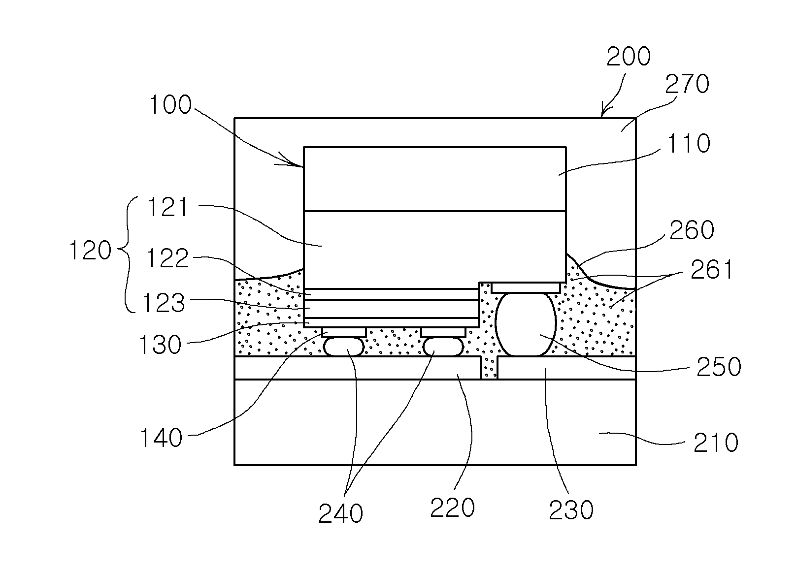
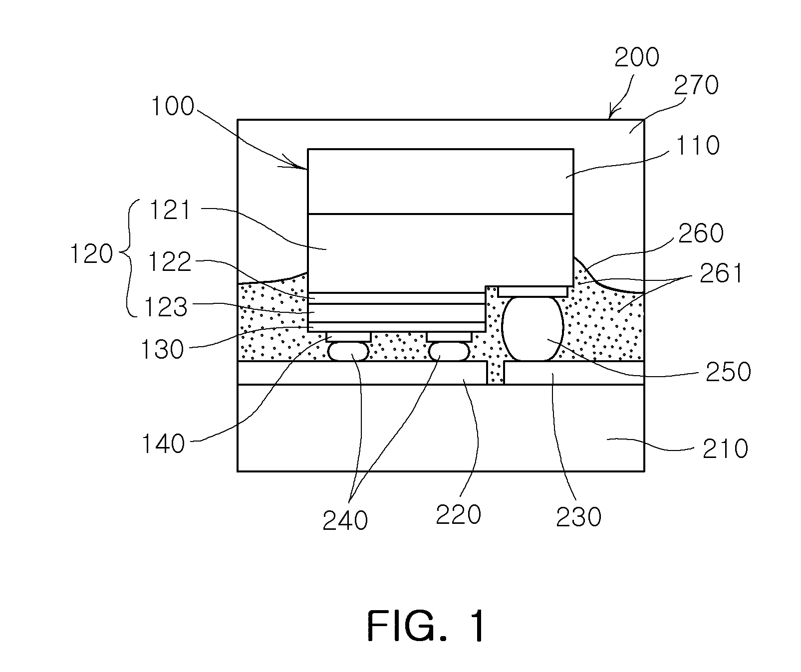
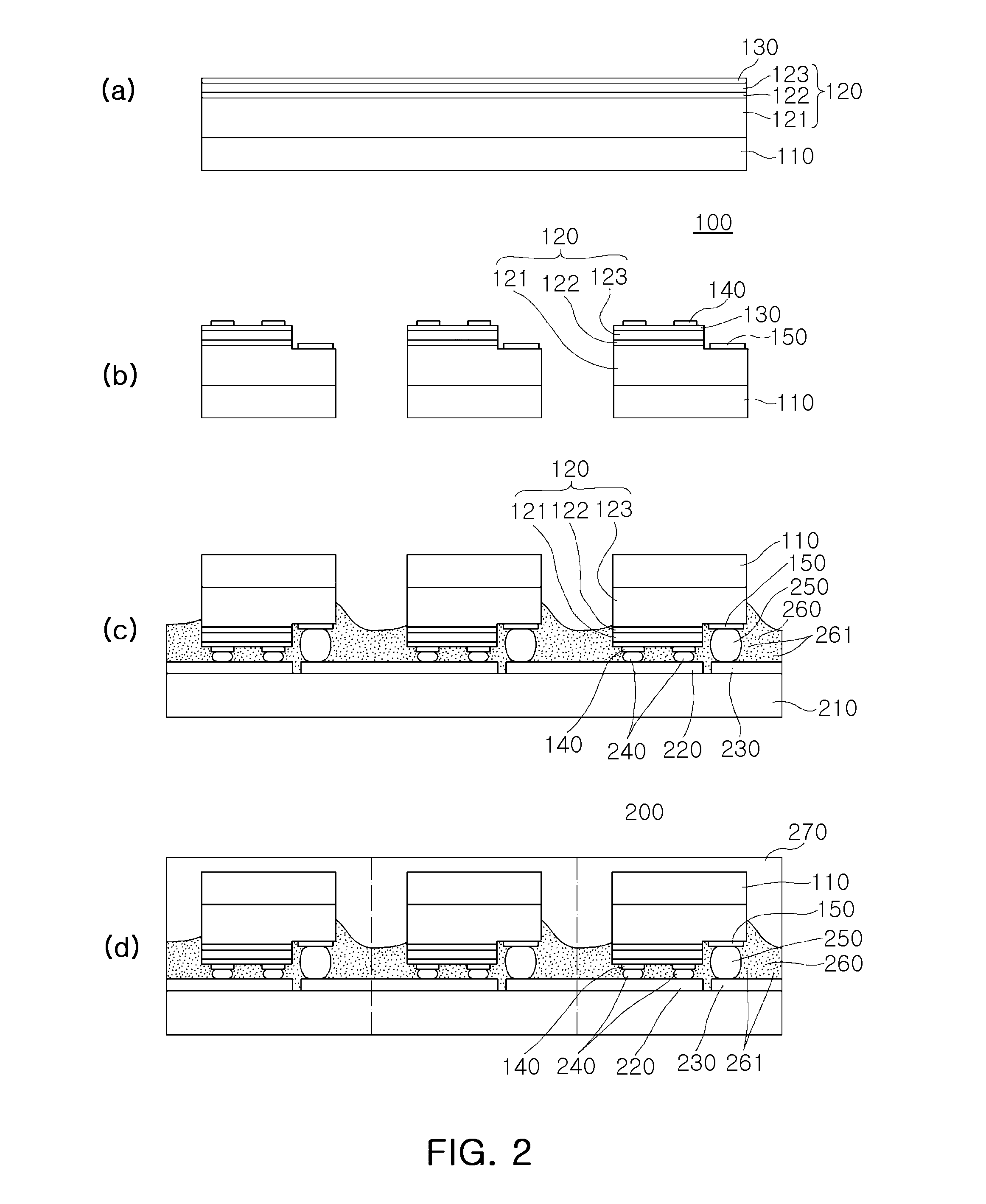
[0030]FIG. 1 is a side sectional view schematically showing a light emitting device package according to a first exemplary embodiment of the present invention. Here, the first exemplary embodiment of the present invention is a light emitting device package having a structure in which a light emitting device is flipchip-bonded. In this case, the light emitting device has a st...


PUM


Abstract

A light emitting device package includes: a substrate with a mounting surface; a light emitting device bonded to the mounting surface of the substrate; a light reflecting resin part containing a high reflective material, filled on the substrate around the light emitting device so as to extend in a space between the light emitting device and the substrate; and a packing resin part hermetically sealed to cover the light emitting device and the light reflection resin part.

Description

TECHNICAL FIELD[0001]The present invention relates to a light emitting device package and, more particularly, to a light emitting device package capable of improving luminous efficiency, and a fabricating method thereof.BACKGROUND ART[0002]Recently, a nitride light emitting device, a light emitting diode for acquiring light of a blue or green wavelength range, is fabricated with a semiconductor material having an empirical formula of AlxInyGa(1-x-y)N (here, 0≦x≦1, 0≦y≦1, 0≦x+y≦1). As such an LED has various advantages such as along life span, low power consumption, good initial driving characteristics, high vibration resistance, and the like, compared with a light emitting device based on a filament, demand for the LED continues to increase, and the recent active development of a high output LED promotes the use of the LED in diverse application fields such as an automobile light source, an electronic board, illumination, a light source for a backlight unit of a display, and the lik...

Claims


Application Information

Patent Timeline
IPC IPC(8): H01L33/60
CPCH01L33/56H01L33/54H01L33/60H01L2924/181H01L24/97H01L2224/32245H01L2224/48091H01L2224/48247H01L2224/49107H01L2224/73204H01L2224/73265H01L2224/8592H01L2224/14H01L2224/97H01L2924/00014H01L2924/00012H01L2924/00H01L33/52
Inventor KIM, JIN HANEI, MASAMIHWANG, SEOK MINJEON, CHUNG BAE
Owner SAMSUNG ELECTRONICS CO LTD
Why Eureka
Try Eureka