

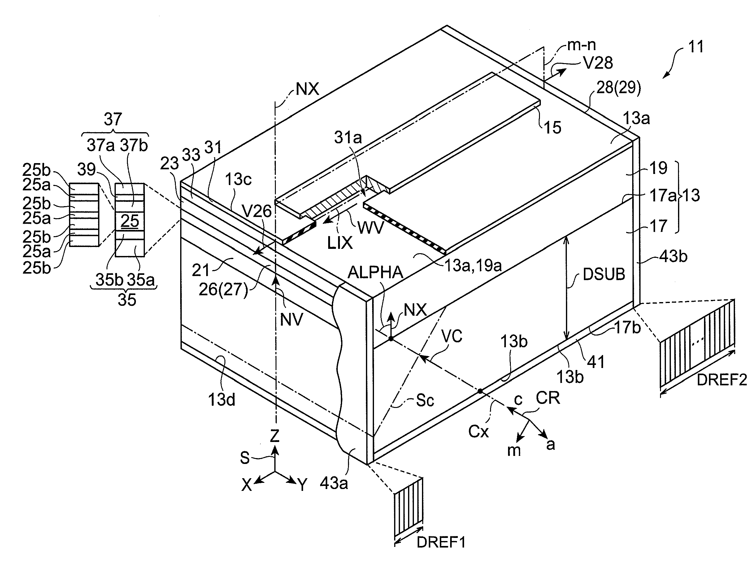
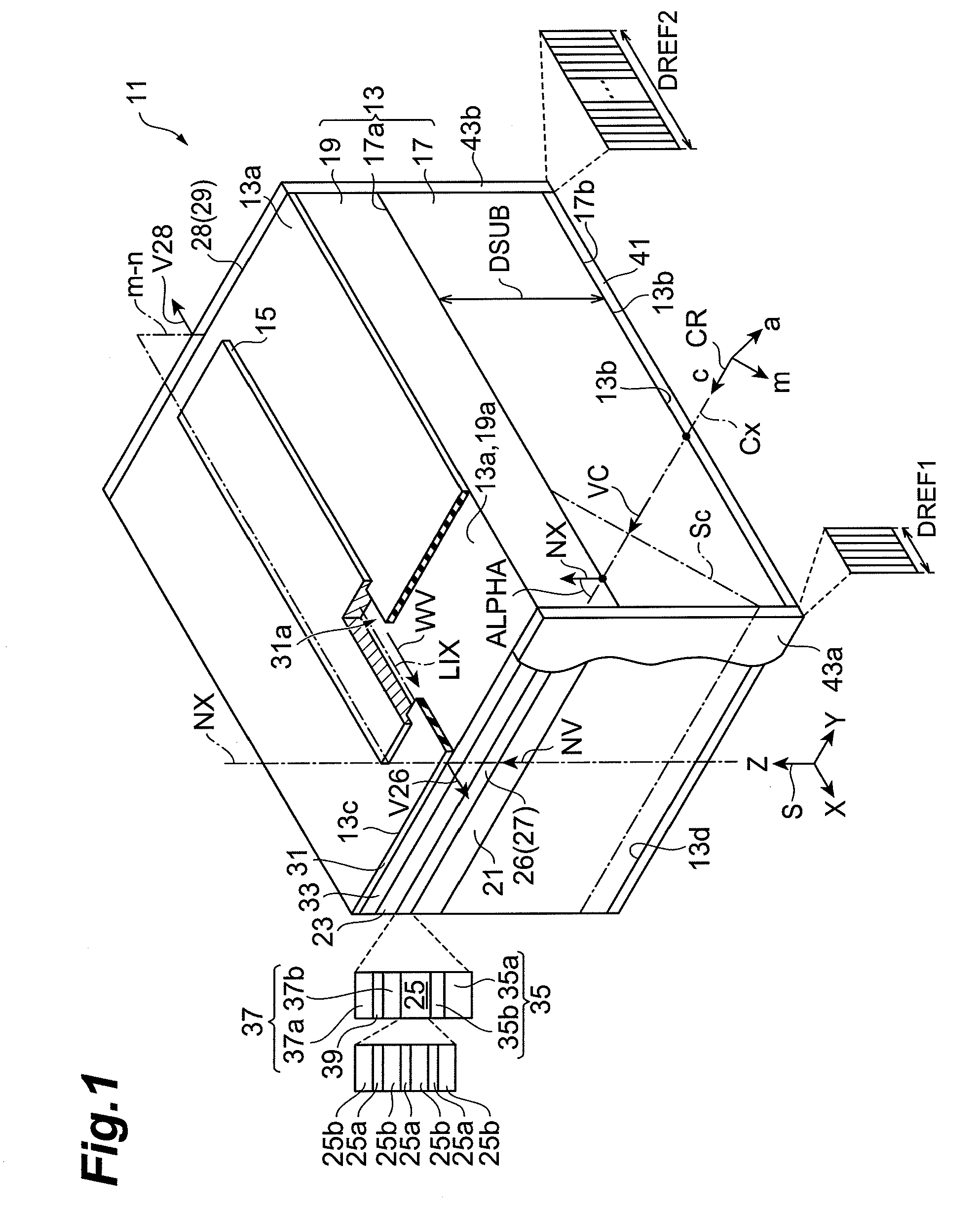
Iii-intride semiconductor laser device, and method of fabricating the iii-nitride semiconductor laser device
a laser device and semiconductor technology, applied in semiconductor devices, lasers, semiconductor lasers, etc., can solve problems such as catastrophic optical damage (cod) and achieve the effect of improving cod level and reducing optical absorption
- Summary
- Abstract
- Description
- Claims
- Application Information
AI Technical Summary
Benefits of technology
Problems solved by technology
Method used
Image

Examples
example 1
[0155]A laser diode is grown by organometallic vapor phase epitaxy as described below. Raw materials used are as follows: trimethyl gallium (TMGa); trimethyl aluminum (TMAl); trimethyl indium (TMIn); ammonia (NH3); silane (SiH4); and bis(cyclopentadienyl) magnesium (Cp2Mg). A substrate 71 is prepared, which is a {20-21} GaN substrate. This GaN substrate is fabricated by cutting a (0001) GaN ingot, grown thick by HYPE, with a wafer slicing apparatus at an angle of 75 degrees with respect to the m-axis direction.
[0156]This substrate is loaded into a susceptor in a growth reactor, and thereafter epitaxial layers for the laser structure shown in FIG. 7 are grown through the following growth procedure. After the substrate 71 is set in the growth reactor, an n-type GaN layer (thickness: 1000 nm) 72 is first grown on the substrate 71. Next, an n-type InAlGaN cladding layer (thickness: 1200 nm) 73 is grown on the n-type GaN layer 72. Subsequently, the light emitting layer is formed. First, ...
example 2
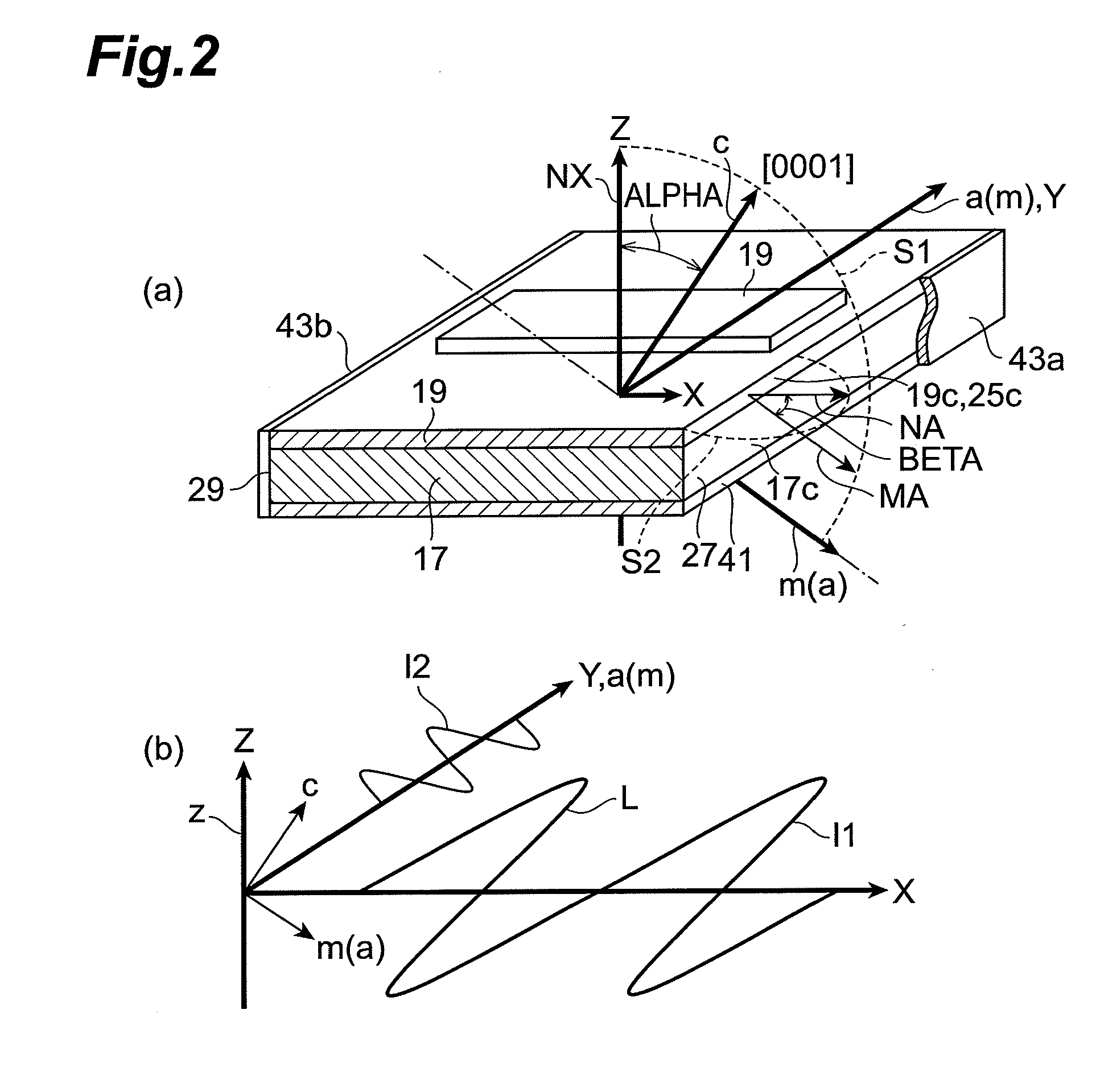
[0183]The below provides plane indices of primary surfaces of GaN substrates and plane indices perpendicular to the primary surfaces of substrates and nearly perpendicular to the direction of the projected c-axis onto the primary surface. The unit of angle is “degree.”
Plane index of primary surface: Angle to (0001), Plane index of first end face perpendicular to primary surface, Angle to primary surface.[0184](0001): 0.00, (−1010), 90.00; part (a) of FIG. 11.[0185](10-17): 15.01, (−2021), 90.10; part (b) of FIG. 11.[0186](10-12): 43.19, (−4047), 90.20; part (a) of FIG. 12.[0187](10-11): 61.96, (−2027), 90.17; part (b) of FIG. 12.[0188](20-21): 75.09, (−1017), 90.10; part (a) of FIG. 13.[0189](10-10): 90.00, (0001), 90.00; part (b) of FIG. 13.[0190](20-2-1): 104.91, (10-17), 89.90; part (a) of FIG. 14.[0191](10-1-1): 118.04, (20-27), 89.83; part (b) of FIG. 14.[0192](10-1-2): 136.81, (40-47), 89.80; part (a) of FIG. 15.[0193](10-1-7): 164.99, (20-21), 89.90; part (b) of FIG. 15.[0194...
PUM
 Abstract
Description
Claims
Application Information