P-Type Semiconductor Material and Semiconductor Device

a semiconductor material and semiconductor technology, applied in the direction of semiconductor devices, basic electric elements, electrical appliances, etc., can solve the problems of reducing the output current of power generation, reducing the output current by contraries, and unable to obtain the output current as high, so as to improve the p-n heterojunction interface, reduce light absorption loss, and facilitate photocurrent carrier extraction

Inactive Publication Date: 2013-08-22
SEMICON ENERGY LAB CO LTD
View PDF1 Cites 20 Cited by
  • Summary
  • Abstract
  • Description
  • Claims
  • Application Information

AI Technical Summary

Benefits of technology

[0051]According to one embodiment of the present invention, an oxide semiconductor material having p-type conductivity can be provided. Alternatively, a semiconductor device using the oxide semiconductor material can be provided. Examples of the semiconductor device include a transistor, a diode, a photoelectric conversion device, an electro-optical device, a light-emitting display device, a memory device, an imaging device, a semiconductor circuit, and an electronic device. Alternatively, a semiconductor device with low light absorption los

Problems solved by technology

In that case, the conduction of photocarriers is blocked by the barrier, so that there is a difficulty in taking the photocarriers out; thus, output current is reduced by contraries.
Thus, there is a problem in that the output current in power generation cannot be obtained as high as the theoretical value even in the cas

Method used


Image

  • P-Type Semiconductor Material and Semiconductor Device
  • P-Type Semiconductor Material and Semiconductor Device
  • P-Type Semiconductor Material and Semiconductor Device

Examples


embodiment 1

[0086]In this embodiment, an oxide semiconductor material that is one embodiment of the disclosed invention is described with reference to FIG. 1, FIG. 2, FIG. 3, and FIG. 5.

[0087]As the oxide semiconductor material of one embodiment of the present invention, molybdenum oxide can be used. Molybdenum oxide is preferable since it is stable even in air, has a low hygroscopic property, and is easily treated. Further, oxides of metals that belong to Group 4 to Group 8 of the periodic table can also be used. Specific examples thereof include vanadium oxide, niobium oxide, tantalum oxide, chromium oxide, tungsten oxide, manganese oxide, and rhenium oxide.

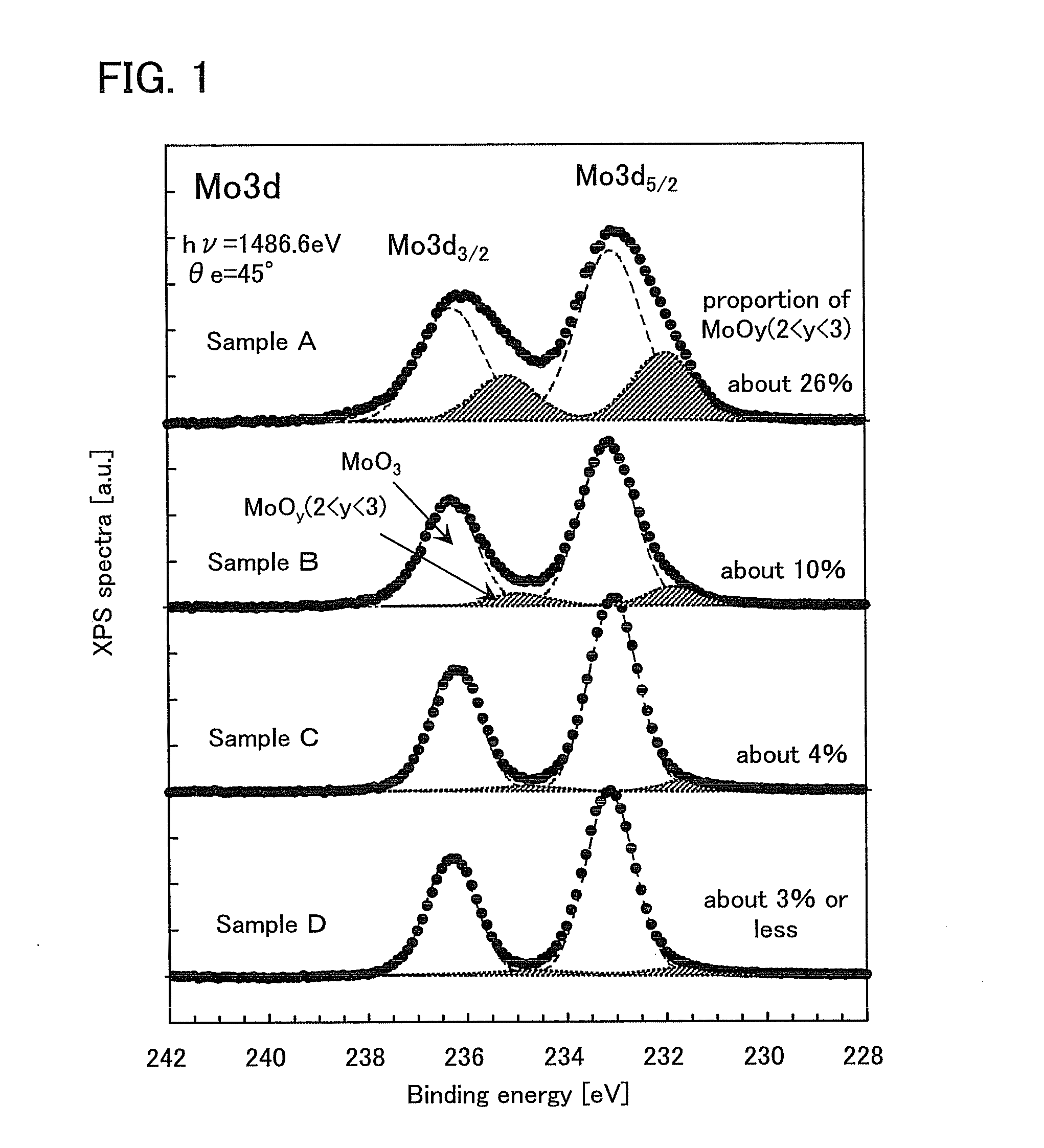
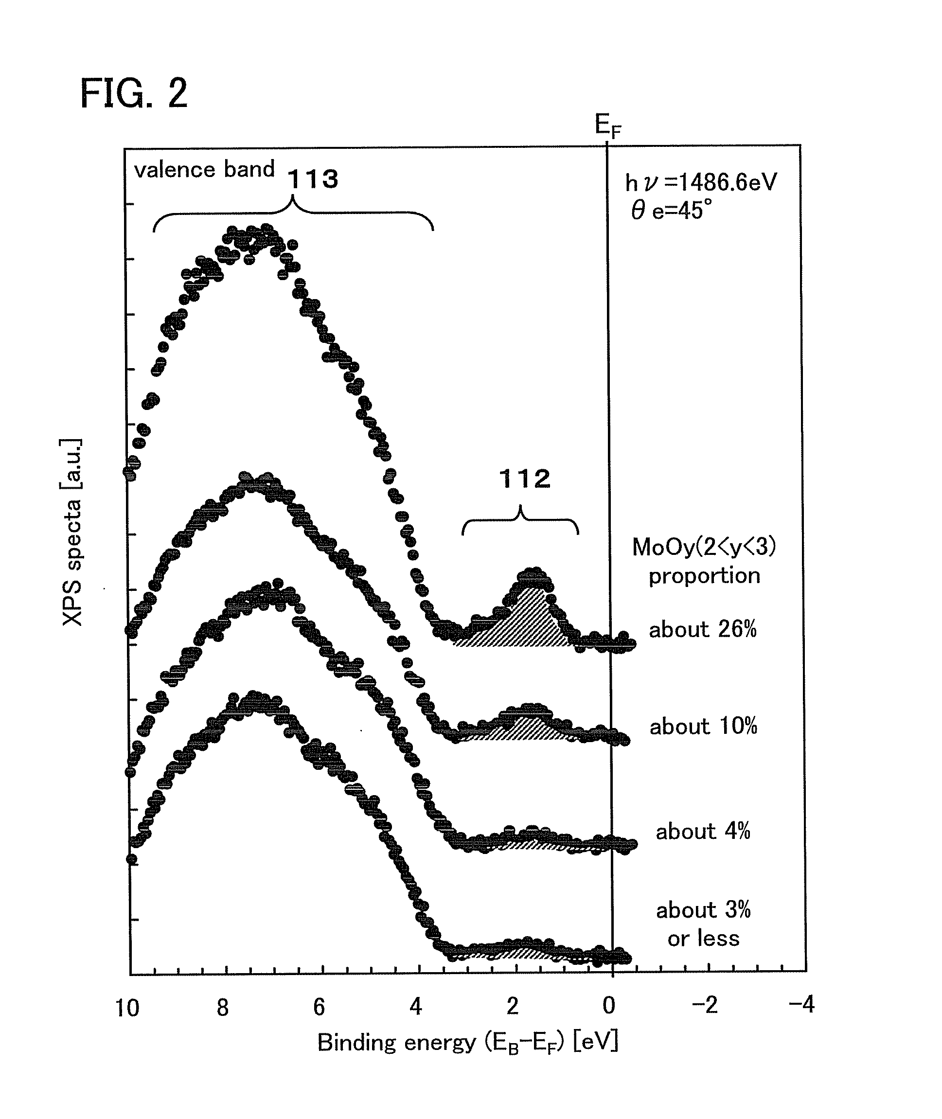
[0088]As molybdenum oxide of the oxide semiconductor material, a material (hereinafter referred to as MoO3+MoOy (23) and molybdenum oxide (hereinafter referred to as MoOy (2

[0089]The conductivity of MoO3+MoOy (2y (23+Mo...

embodiment 2

[0113]In this embodiment, a structure of a photoelectric conversion device of one embodiment of the disclosed invention and a manufacturing method thereof are described with reference to FIGS. 6A and 6B, FIGS. 7A and 7B, FIGS. 8A to 8C, and FIGS. 9A to 9C.

[0114]First, a structure of a photoelectric conversion device that is one embodiment of the present invention is described.

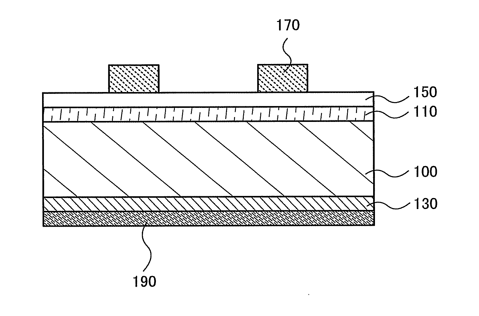
[0115]FIG. 6A shows an example of a schematic cross-sectional view of the photoelectric conversion device that is one embodiment of the present invention. The photoelectric conversion device includes a silicon substrate 100; an oxide semiconductor layer 110 over one surface of the silicon substrate; an impurity region 130 over the other surface of the silicon substrate; a light-transmitting conductive film 150 over the oxide semiconductor layer 110; a first electrode 170 in contact with the light-transmitting conductive film; and a second electrode 190 in contact with the impurity region 130. Note that the firs...

embodiment 3

[0153]In this embodiment, a photoelectric conversion device whose structure is different from the structures of the photoelectric conversion devices in Embodiment 2, and a method for manufacturing the photoelectric conversion device is described with reference to FIG. 10, FIG. 11, FIG. 12, FIG. 13, FIGS. 14A to 14C, and FIGS. 15A to 15C. Note that detailed description of portions which are similar to those of Embodiment 2 is omitted in this embodiment.

[0154]FIG. 10 is a cross-sectional view of a photoelectric conversion device that is one embodiment of the present invention. The photoelectric conversion device includes a silicon substrate 200; a first silicon semiconductor layer 201, an oxide semiconductor layer 210, a light-transmitting conductive film 250, and a first electrode 270 which are formed over one surface of the silicon substrate 200; and a second silicon semiconductor layer 202, a third silicon semiconductor layer 203, and a second electrode 290 which are formed over th...


PUM


Abstract

An oxide semiconductor material having p-type conductivity and a semiconductor device using the oxide semiconductor material are provided. The oxide semiconductor material having p-type conductivity can be provided using a molybdenum oxide material containing molybdenum oxide (MoOy (2<y<3)) having an intermediate composition between molybdenum dioxide and molybdenum trioxide. For example, a semiconductor device is formed using a molybdenum oxide material containing molybdenum trioxide (MoO3) as its main component and MoOy (2<y<3) at 4% or more.

Description

BACKGROUND OF THE INVENTION[0001]1. Field of the Invention[0002]The present invention relates to an object, a method, a method for producing an object, a process, a machine, manufacture, or a composition of matter. In particular, the present invention relates to, for example, a semiconductor device, a display device, a light-emitting device, a driving method thereof, or a manufacturing method thereof. More particularly, the present invention relates to, for example, a semiconductor material and a semiconductor device using the semiconductor material.[0003]In this specification, a “semiconductor device” generally refers to a device which can function by utilizing semiconductor characteristics; a transistor, a diode, a photoelectric conversion device, an electro-optical device, a light-emitting display device, a memory device, an imaging device, a semiconductor circuit, and an electronic device are all included in the category of the semiconductor device.[0004]2. Description of the Re...

Claims


Application Information

Patent Timeline
IPC IPC(8): H01L29/20
CPCH01L31/074Y02E10/50H01L29/7869H01L29/267H01L29/20H01L29/861H01L31/0328
Inventor ASAMI, YOSHINOBUKATAISHI, RIHOKIKUCHI, ERUMU
Owner SEMICON ENERGY LAB CO LTD
Why Eureka
Try Eureka