Silicon-based lateral injection laser and preparation method thereof

A laser and lateral technology, applied in the field of silicon-based lateral injection lasers and their preparation, can solve the problems of large lasing threshold of devices, complex germanium materials, large optical loss, etc., to reduce optical absorption loss, simplify process steps, and improve compatibility. sexual effect

Active Publication Date: 2019-02-15
INST OF SEMICONDUCTORS - CHINESE ACAD OF SCI
View PDF4 Cites 0 Cited by
  • Summary
  • Abstract
  • Description
  • Claims
  • Application Information

AI Technical Summary

Problems solved by technology

The silicon-based germanium laser designed by MIT and the University of Stuttgart in Germany has a vertical p-n structure, and the absorption of light by the doped layer and the electrode is not well avoided. The sidewall of the waveguide formed by etching has a large optical loss, and it is necessary to use complex materials that are not very sensitive to germanium. Mature chemical mechanical polishing process and other issues
Due to the large optical loss of the waveguide, the consistency of the device is not good, the lasing threshold of the device is too large, the life is very short, and continuous operation cannot be achieved.

Method used


Image

  • Silicon-based lateral injection laser and preparation method thereof
  • Silicon-based lateral injection laser and preparation method thereof
  • Silicon-based lateral injection laser and preparation method thereof

Examples


Embodiment Construction

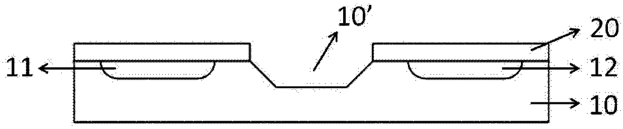
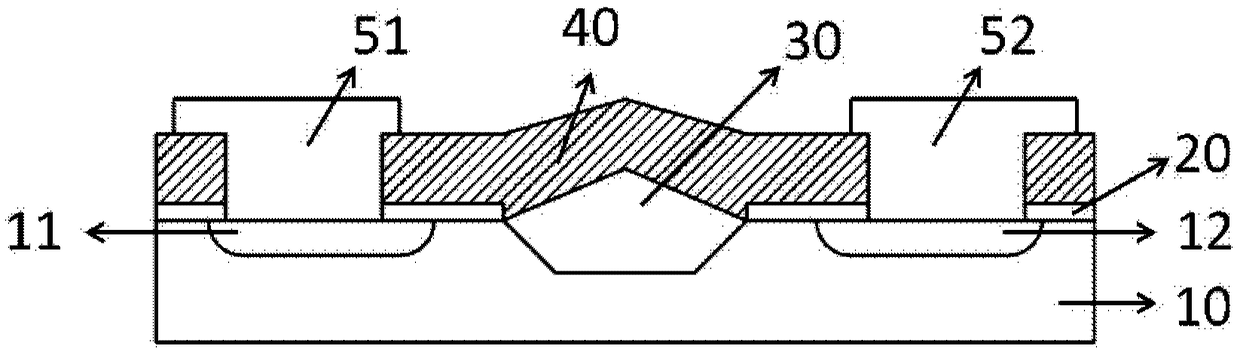
[0029] see figure 1 , figure 2 As shown, the invention provides a silicon-based lateral injection laser, comprising:

[0030] A silicon substrate 10 has a waveguide groove 10' fabricated on its surface, and p-type doped regions 11 and n-type doped regions 12 are respectively fabricated on both sides of the waveguide groove 10'. The silicon substrate 10 has a (001) crystal orientation, wherein the waveguide trenches 10' extend along the (110) crystal orientation. If the waveguide groove 10' is formed by selective wet etching, the sidewall of the waveguide groove 10' is a (111) crystal plane, and the smooth sidewall can reduce the gap between the strip waveguide 30 and the sidewall of the waveguide groove 10'. light scattering loss; if etching or non-selective etching is used to form the waveguide trench 10', the sidewall of the waveguide trench 10' generally does not have a strictly specific crystal orientation, and the smoothness of the sidewall is not as good as using sele...


PUM


Abstract

The invention provides a silicon-based horizontal injection laser and a preparation method thereof. The silicon-based horizontal injection laser comprises a silicon substrate, a silicon dioxide window layer, a strip waveguide, an insulating medium layer, a p electrode and an n electrode, wherein a waveguide groove is manufactured in the middle of the upper surface of the silicon substrate; a p-type doped region and an n-type doped region are formed in two sides of the waveguide groove in the upper surface of the silicon substrate; the silicon dioxide window layer is manufactured on one part of the surface of the silicon substrate; side windows are formed in the upper surface, corresponding to the p-type doped region and the n-type doped region, of the silicon dioxide window layer separately; the strip waveguide grows in the waveguide groove of the silicon substrate; the insulating medium layer is manufactured on the surface of the strip waveguide and covers the surface of the silicon dioxide window layer; the p electrode is manufactured in one side window in the silicon dioxide window layer in the P-type doped region; and the n electrode is manufactured in the other side window in the silicon dioxide window layer in the n-type doped region. By the silicon-based horizontal injection laser, the compatibility of the silicon-based horizontal injection laser and a silicon CMOS process can be improved.

Description

technical field [0001] The invention relates to the technical field of semiconductor lasers, in particular to a silicon-based lateral injection laser and a preparation method thereof. technical background [0002] With the integration of silicon integrated circuits getting higher and higher and the speed of information transmission getting faster and faster, the traditional electrical interconnection has shown its technical limitations and cannot meet the needs of high bandwidth and low power consumption. Optical interconnection has the characteristics of high speed, high bandwidth, and low power consumption. Therefore, people are eager to realize optical interconnection in a short distance, even silicon-based optical interconnection between chips and inside chips. Among the most important basic devices in silicon-based optical interconnection, except for silicon-based light sources, other devices can be realized under the current silicon process conditions. This makes effi...

Claims


Application Information

Patent Timeline
Patent Type & Authority Patents(China)
IPC IPC(8): H01S5/223
CPCH01S5/223
Inventor 刘智成步文李传波薛春来王启明
Owner INST OF SEMICONDUCTORS - CHINESE ACAD OF SCI
Why Eureka
Try Eureka