photoelectric conversion device
A photoelectric conversion device, light-transmitting and conductive technology, applied in photovoltaic power generation, circuits, electrical components, etc., can solve the problems of low conductivity, non-use, and resistance loss of the i-type amorphous semiconductor layer, so as to reduce light absorption loss , reduced resistance loss, high conversion efficiency
- Summary
- Abstract
- Description
- Claims
- Application Information
AI Technical Summary
Problems solved by technology
Method used
Image
Examples
Embodiment approach 1
[0041] In this embodiment mode, a photoelectric conversion device according to one embodiment of the present invention and a method for manufacturing the same will be described.
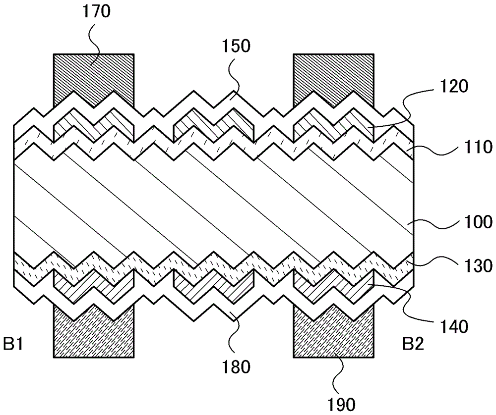
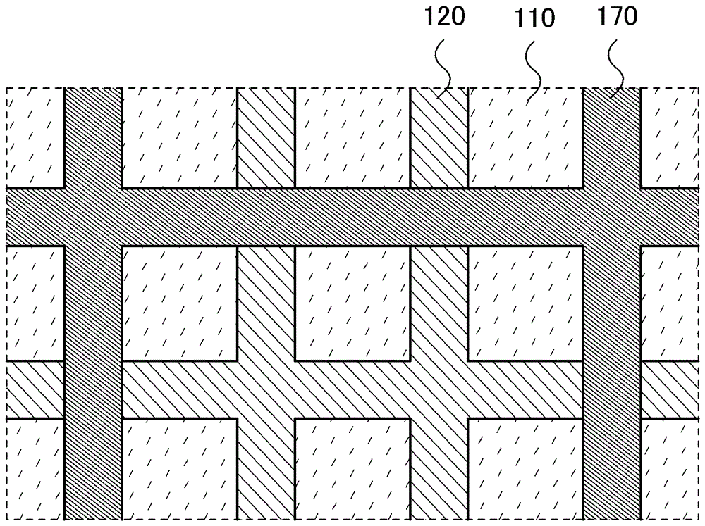
[0042] Figure 1A is a plan view of a photoelectric conversion device in one embodiment of the present invention, Figure 1B is a cross-sectional view along line A1-A2 of the plan view. The photoelectric conversion device includes: a crystalline silicon substrate 100; a first silicon semiconductor layer 110, a second silicon semiconductor layer 120, a light-transmitting conductive film 150, and a first electrode 170 formed on one surface of the crystalline silicon substrate; and The third silicon semiconductor layer 130, the fourth silicon semiconductor layer 140 and the second electrode 190 are formed on the other surface of the crystalline silicon substrate. In addition, the first electrode 170 is a grid electrode, and one side of the first electrode 170 becomes a light receiving surface.
[0043...
Embodiment approach 2
[0098] In this embodiment, a photoelectric conversion device having a different configuration from the photoelectric conversion device described in Embodiment 1 will be described. In addition, regarding the common parts with Embodiment 1, detailed description thereof will be omitted in this embodiment.
[0099] Figure 9 It is a cross-sectional view of a photoelectric conversion device in one embodiment of the present invention. The photoelectric conversion device includes: a crystalline silicon substrate 300 whose surface is processed by embossing; a first silicon semiconductor layer 310 formed on one surface of the crystalline silicon substrate; The first light-transmitting conductive film 410; the second silicon semiconductor layer 320 formed in the opening; the first electrode 370 formed on the second silicon semiconductor layer; and a surface formed on the crystalline silicon substrate covering The second light-transmitting conductive film 420 on the above-mentioned lam...
Embodiment approach 3
[0134] In this embodiment, a photoelectric conversion device having a different configuration from the photoelectric conversion devices described in Embodiments 1 and 2 will be described. In addition, as for the parts common to Embodiments 1 and 2, detailed description thereof will be omitted in this embodiment.
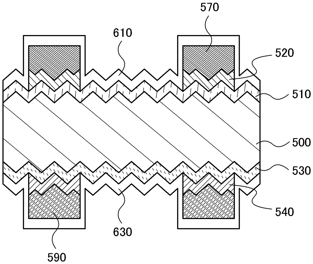
[0135] Figure 13 It is a cross-sectional view of a photoelectric conversion device in one embodiment of the present invention. The photoelectric conversion device includes: a crystalline silicon substrate 500 whose surface has been processed by embossing; a first silicon semiconductor layer 510 formed on one surface of the crystalline silicon substrate; The first electrode 570 formed on the second silicon semiconductor layer; and the light-transmitting film 610 covering the above-mentioned stacked film formed on one surface of the crystalline silicon substrate. In addition, the photoelectric conversion device includes: a third silicon semiconductor layer 530 forme...
PUM
 Abstract
Description
Claims
Application Information


