Method for precision integrated circuit die singulation using differential etch rates

a technology of differential etching rate and integrated circuit die, which is applied in the direction of basic electric elements, semiconductor/solid-state device manufacturing, electric apparatus, etc., can solve the problems that existing dicing means do not provide the necessary accuracy for the above-mentioned applications, and the singulation required cannot meet tolerances

Active Publication Date: 2008-02-26
NYTELL SOFTWARE LLC
View PDF14 Cites 60 Cited by
  • Summary
  • Abstract
  • Description
  • Claims
  • Application Information

AI Technical Summary

Problems solved by technology

Applications where very high tolerance die singulation is required cannot accommodate the tolerances associated with blade dicing or, for that matter, laser dicing.
Existing dicing means do not provide the necessary accuracy for the above applications.

Method used


Image

  • Method for precision integrated circuit die singulation using differential etch rates
  • Method for precision integrated circuit die singulation using differential etch rates
  • Method for precision integrated circuit die singulation using differential etch rates

Examples


Embodiment Construction

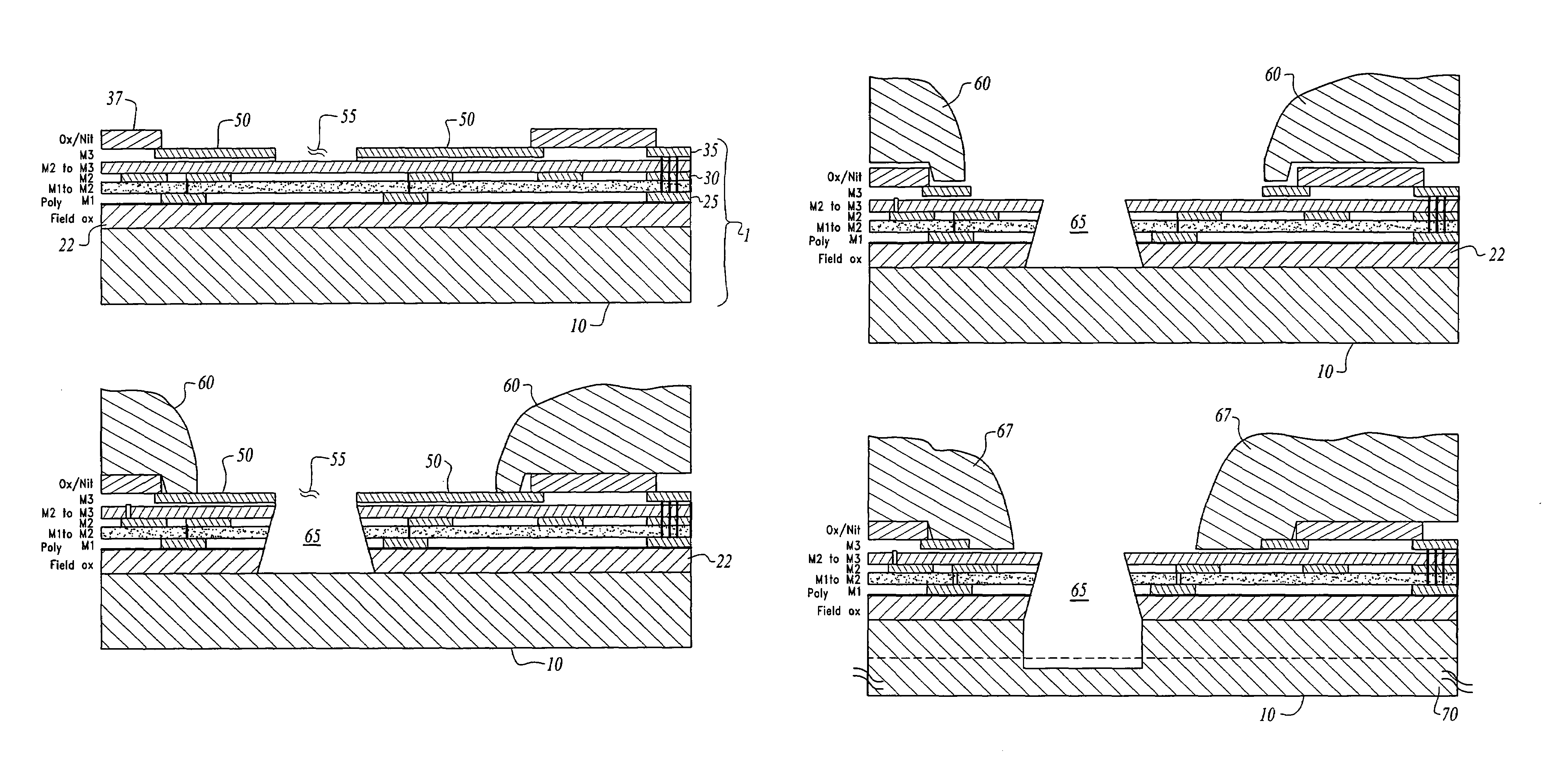
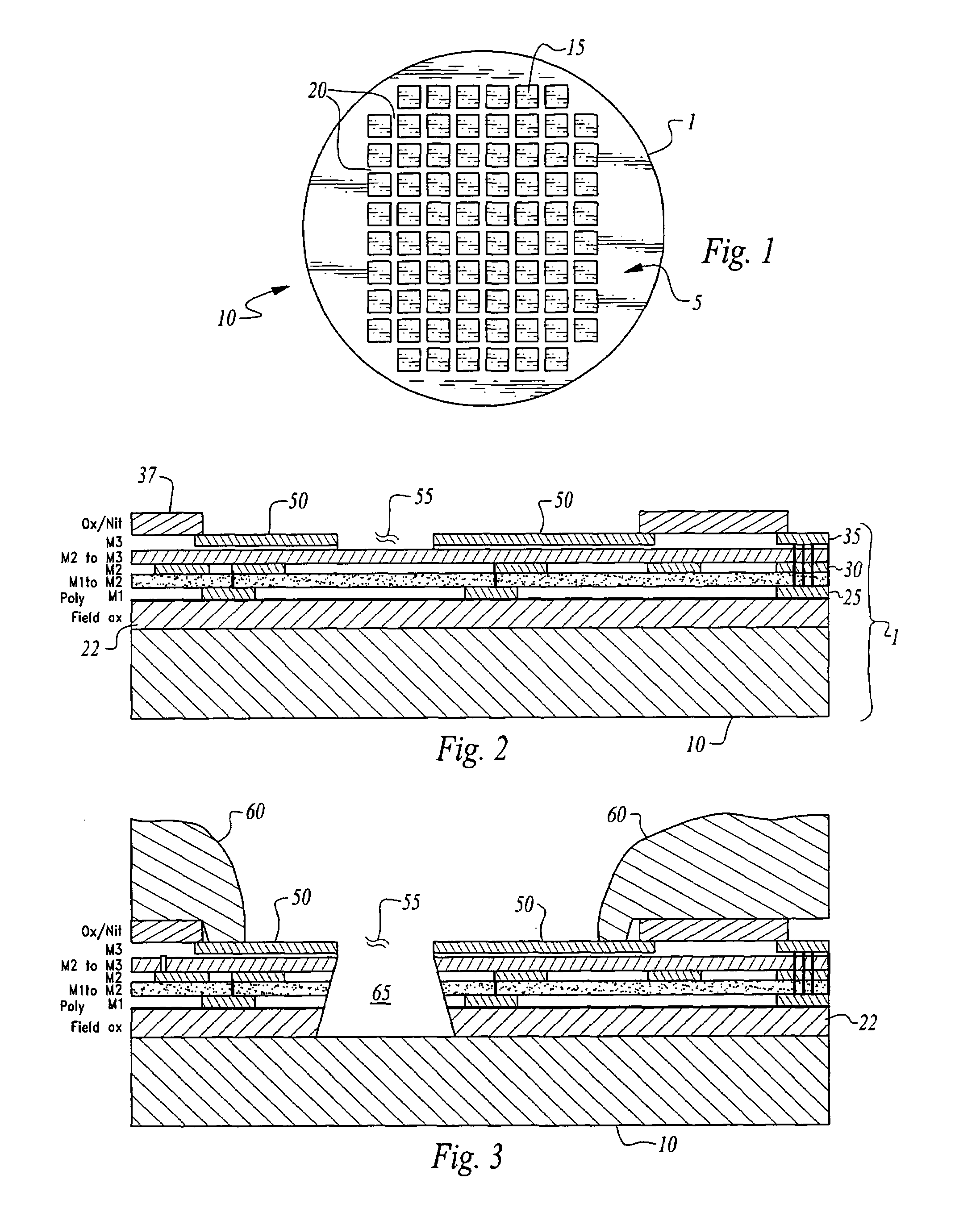
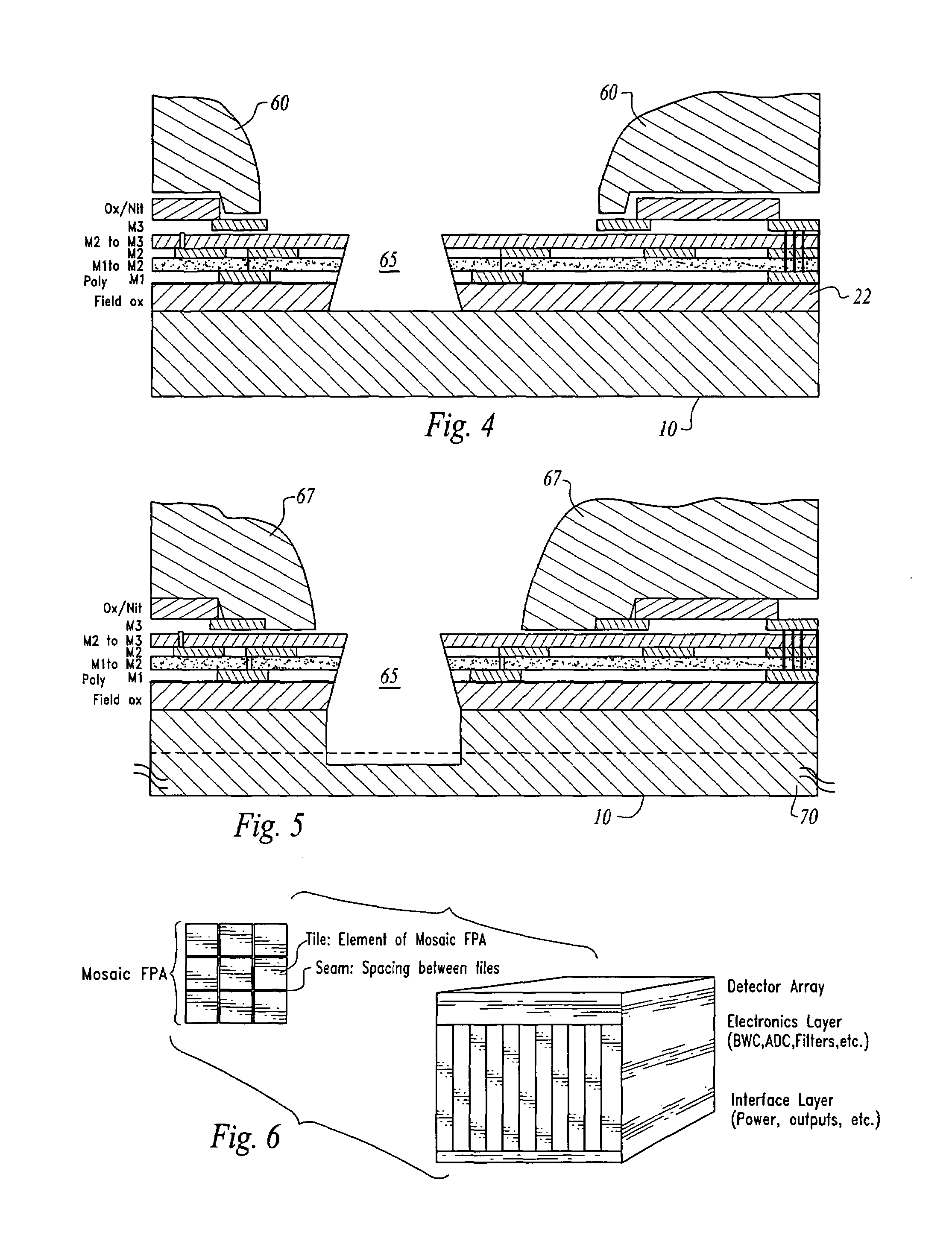
[0026]As is well known in the semiconductor manufacturing arts, a common series of semiconductor process steps is involved in the manufacturing of integrated circuit die.

[0027]Generally, such semiconductor process steps comprise:

[0028]1. Functional and schematic circuit design,

[0029]2. Circuit layout (which is dependent on factors such as feature size, material characteristics and foundry capabilities) resulting in a composite circuit layout or drawing from which individual circuit layer patterns are generated,

[0030]3. Digitizing each layer drawing,

[0031]4. Creating a reticle from each layer drawing comprising an image for directly patterning the image on a wafer or for the generation of a photomask which may comprise multiple reticle images. (Chrome on glass / quartz is a typical reticle construction),

[0032]5. Forming a base field oxide layer on the surface of a semiconductor wafer (also referred to as a substrate herein) to form a protective layer and doping barrier,

[0033]6. Pattern...


PUM


Abstract

A preprocessed semiconductor substrate such as a wafer is provided with a metal etch mask which defines singulation channels on the substrate surface. An isotropic etch process is used to define a singulation channel with a first depth extending into the semiconductor substrate material. A second anisotropic etch process is used to increase the depth of the singulation channel while providing substantially vertical singulation channel sidewalls. The singulation channel can be extended through the depth of the substrate or, in an alternative embodiment, a predetermined portion of the inactive surface of the substrate removed to expose the singulation channels. In this manner, semiconductor die can be precisely singulated from a wafer while maintaining vertical die sidewalls.

Description

CROSS REFERENCE TO RELATED APPLICATIONS[0001]The present application claims priority to U.S. provisional patent application Ser. No. 60 / 628,742, filed Nov. 18, 2004, and U.S. provisional patent application Ser. No. 60 / 617,426, filed Oct. 8, 2004, each of which are incorporated fully herein by reference and to which priority is claimed pursuant to 35 USC 119.STATEMENT REGARDING FEDERALLY SPONSORED RESEARCH AND DEVELOPMENT [0002]N / ABACKGROUND OF THE INVENTION [0003]1. Field of the Invention[0004]The invention relates to semiconductor wafer processing. Specifically the invention relates to a method for the precise singulation of integrated circuit die from a semiconductor substrate.[0005]2. Description of the Prior Art[0006]Semiconductor processing generally comprises multiple photolithographic, etching, plating and doping steps to form an array of individual integrated circuit die on the surface of a semiconductor substrate such as a wafer. Integrated circuit die densities frequently ...

Claims


Application Information

Patent Timeline
Patent Type & Authority Patents(United States)
IPC IPC(8): H01L21/00
CPCH01L21/3065H01L21/30655H01L21/78
Inventor DAVID, LUDWIGYAMAGUCHI, JAMESCLARK, STUARTBOYD, W. ERIC
Owner NYTELL SOFTWARE LLC
Why Eureka
Try Eureka