Memory device and method for fabricating the same

a memory device and memory technology, applied in the field of memory devices, can solve the problems of data retention time decreasing, region susceptible, difficulty in controlling the threshold voltage of the memory device, etc., and achieve the effect of decreasing junction leakage current and increasing data retention tim

Active Publication Date: 2006-05-16
SK HYNIX INC
View PDF8 Cites 17 Cited by
  • Summary
  • Abstract
  • Description
  • Claims
  • Application Information

AI Technical Summary

Benefits of technology

[0008]It is, therefore, an object of the present invention to provide a memory device capable of increasing a data retention time by decreasing a junction leakage current created at a storage node contact junction and a method for fabricating the same.

Problems solved by technology

However, the convention memory device has a problem of a short channel effect in that a channel region is susceptible to a voltage provided from the gate structures, depletion layers of the source and drain junctions, an electric field and an electric potential because of the shortened gate electrode.
As a result of the disadvantageous short channel effect, a threshold voltage decreases drastically, thereby resulting in a difficulty in controlling the threshold voltage of the memory device.
The increase in the junction leakage current causes a data retention time to decrease.

Method used


Image

  • Memory device and method for fabricating the same
  • Memory device and method for fabricating the same
  • Memory device and method for fabricating the same

Examples


first embodiment

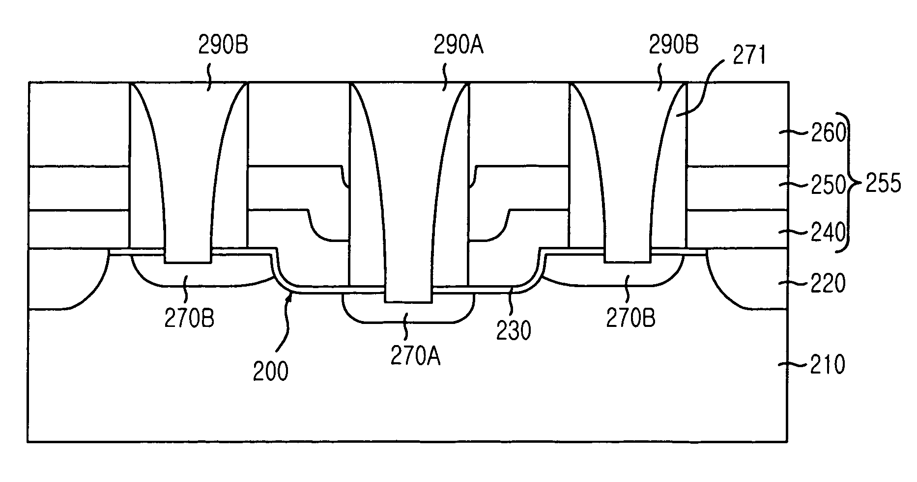
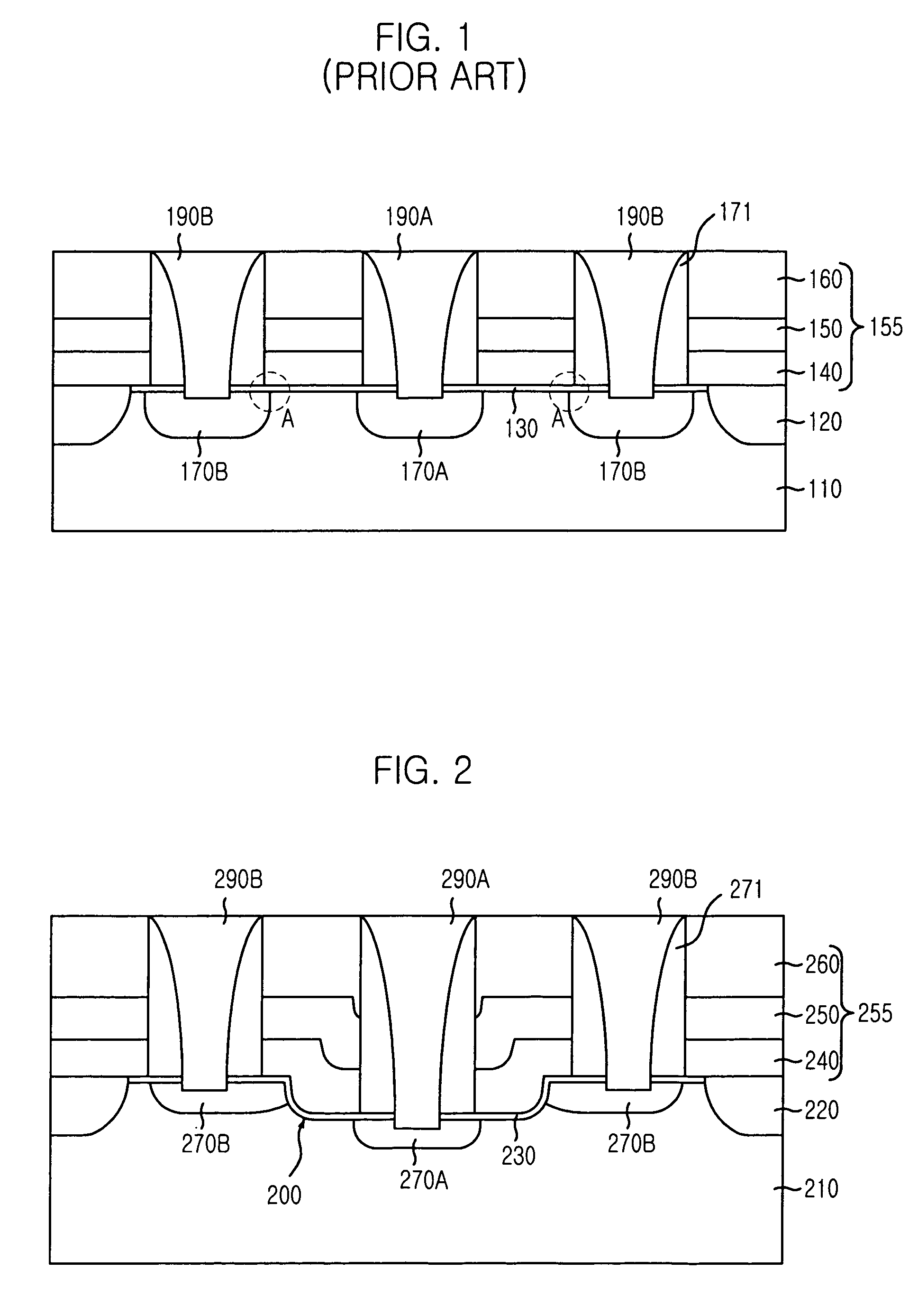
[0023]FIG. 2 is a cross-sectional view showing a structure of a memory device in accordance with the present invention.

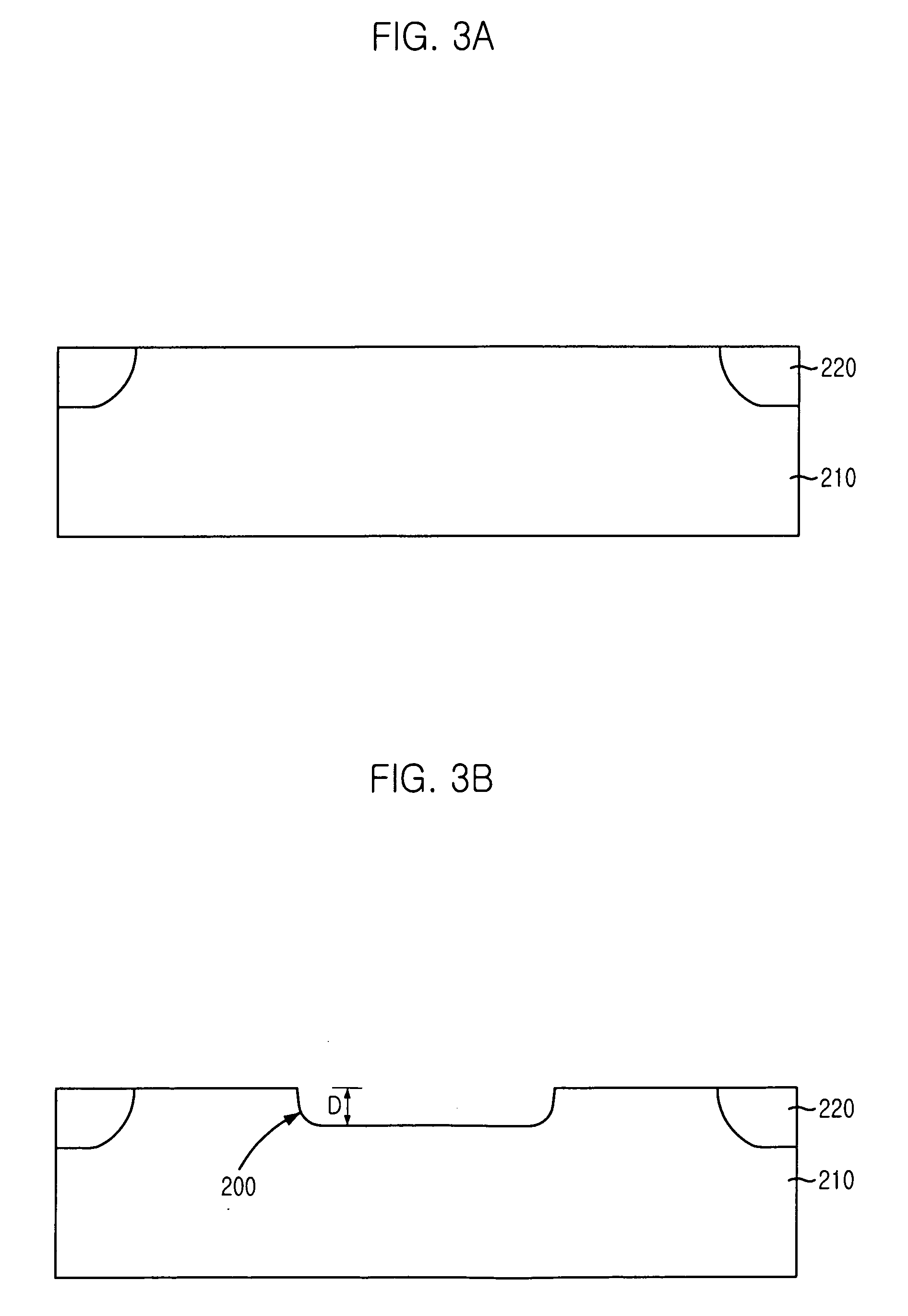
[0024]As shown, a field oxide layer 220 is formed in a substrate 210, and a trench 200 is formed in a predetermined region of the substrate 210. A first contact junction 270A is formed in the substrate 210 disposed beneath the trench 200, while a plurality of second contact junctions 270B are formed in the substrate 210 disposed outside the trench 200. It should be noted that only the single first contact junction 270A is illustrated in FIG. 2 although a number of the first contact junctions 270A are formed.

[0025]A plurality of gate structures 255 are formed on portions of the substrate 210 each disposed between the first contact junction 270A and the second contact junction 270B. Herein, each of the gate structures 255 includes a first insulation layer 230, a polysilicon layer 240, a metal layer 250 and a second insulation layer 260 for use in a hard mask. Also, on...

second embodiment

[0038]FIG. 4 is a cross-sectional view showing a structure of a memory device in accordance with the present invention.

[0039]Herein, the memory device in accordance with the second embodiment includes the same configuration elements described in FIG. 2, and thus, a detailed description of such configuration elements will be omitted. However, the memory device fabricated in accordance with the second embodiment is different from the memory device fabricated in accordance with the first embodiment in that sidewalls B of a trench 300 are formed to be perpendicular to a surface of the indented portion of the substrate 310 and a plurality of gate structures 355, a first contact junction 370A and a second contact junction 370B are disposed such that portions of the substrate 310 where the sidewalls B of the trench 300 are disposed are allocated in the center of the individual channel regions.

third embodiment

[0040]FIG. 5 is a cross-sectional view showing a structure of a memory device in accordance with the present invention.

[0041]Herein, the memory device in accordance with the third embodiment of the present invention includes the same configuration elements described in FIG. 2 and thus, a detailed description of such configuration elements will be omitted. However, the memory device fabricated in accordance with the third embodiment is different from the memory device shown in FIG. 2 in that sidewalls C of a trench 400 are positively sloped by being narrowed down going towards a bottom portion of the trench 400.


PUM


Abstract

Disclosed are a memory device and a method for fabricating the same. The memory device includes: a substrate provided with a trench; a bit line contact junction formed beneath the trench; a plurality of storage node contact junctions formed outside the trench; and a plurality of gate structures each being formed on the substrate disposed between the bit line contact junction and one of the storage node contact junctions. Each sidewall of the trench becomes a part of the individual channels and thus, channel lengths of the transistors in the cell region become elongated. Accordingly, the storage node contact junctions have a decreased level of leakage currents, thereby increasing data retention time.

Description

FIELD OF THE INVENTION[0001]The present invention relates to a memory device and a method for fabricating the same; and more particularly, to a memory device capable of improving a data retention time and a method for fabricating the same.DESCRIPTION OF RELATED ARTS[0002]As semiconductor devices have been increasingly scaled down, each pattern size has been decreased gradually. Particularly, in a memory device such as a dynamic random access memory (DRAM) device, lengths of gate electrodes have been dramatically decreased in proportion to a decrease in sizes of transistors in a cell region owing to the large scale of integration, and as a result of the scaled down gate electrodes, source and drain junctions have played an important role for an electric field and an electric potential exerted on bodies of the transistors in the cell region.[0003]FIG. 1 is a cross-sectional view showing a structure of a conventional memory device.[0004]As shown, a field oxide layer 120 for isolating d...

Claims


Application Information

Patent Timeline
Patent Type & Authority Patents(United States)
IPC IPC(8): H01L27/108
CPCH01L27/10855H01L27/10888H01L29/7886H01L27/11521H01L27/115H10B12/0335H10B12/485H10B69/00H10B41/30
Inventor JANG, SE-AUGJUNG, TAE-WOOKIM, SEO-MINKIM, WOO-JINPARK, HYUNG-SOONKIM, YOUNG-BOGYANG, HONG-SEONSOHN, HYUN-CHULHWANG, EUNG-RIM
Owner SK HYNIX INC
Why Eureka
Try Eureka