Recessed channel transistor and method for preparing the same

a recessed channel transistor and channel transistor technology, applied in transistors, electrical devices, semiconductor devices, etc., can solve the problems of significant gate induced drain leakage current in the recessed channel transistor, and achieve the effects of reducing drain leakage current, enhancing data retention time, and reducing leakage current fluctuation

Active Publication Date: 2010-08-24
PROMOS TECH INC
View PDF20 Cites 3 Cited by
  • Summary
  • Abstract
  • Description
  • Claims
  • Application Information

AI Technical Summary

Benefits of technology

[0009]One aspect of the present invention provides a recessed channel transistor with elevated doped regions serving as source and drain and a method for preparing the same, which can reduce drain leakage current and also reduce the fluctuation of leakage current to enhance the data retention time.
[0012]The conventional recessed channel transistor exhibits a significant gate induced drain leakage current due to the large overlap between the recessed gate and the source / drain regions. In contrast, the source / drain regions of the recessed channel transistor are positioned above the recessed gate; therefore, the gate induced drain leakage current due to the overlap between the recessed gate and the source / drain regions can be dramatically decreased according to the present invention.

Problems solved by technology

The conventional recessed channel transistor exhibits a significant gate induced drain leakage current due to the large overlap between the recessed gate and the source / drain regions.

Method used


Image

  • Recessed channel transistor and method for preparing the same
  • Recessed channel transistor and method for preparing the same
  • Recessed channel transistor and method for preparing the same

Examples


Embodiment Construction

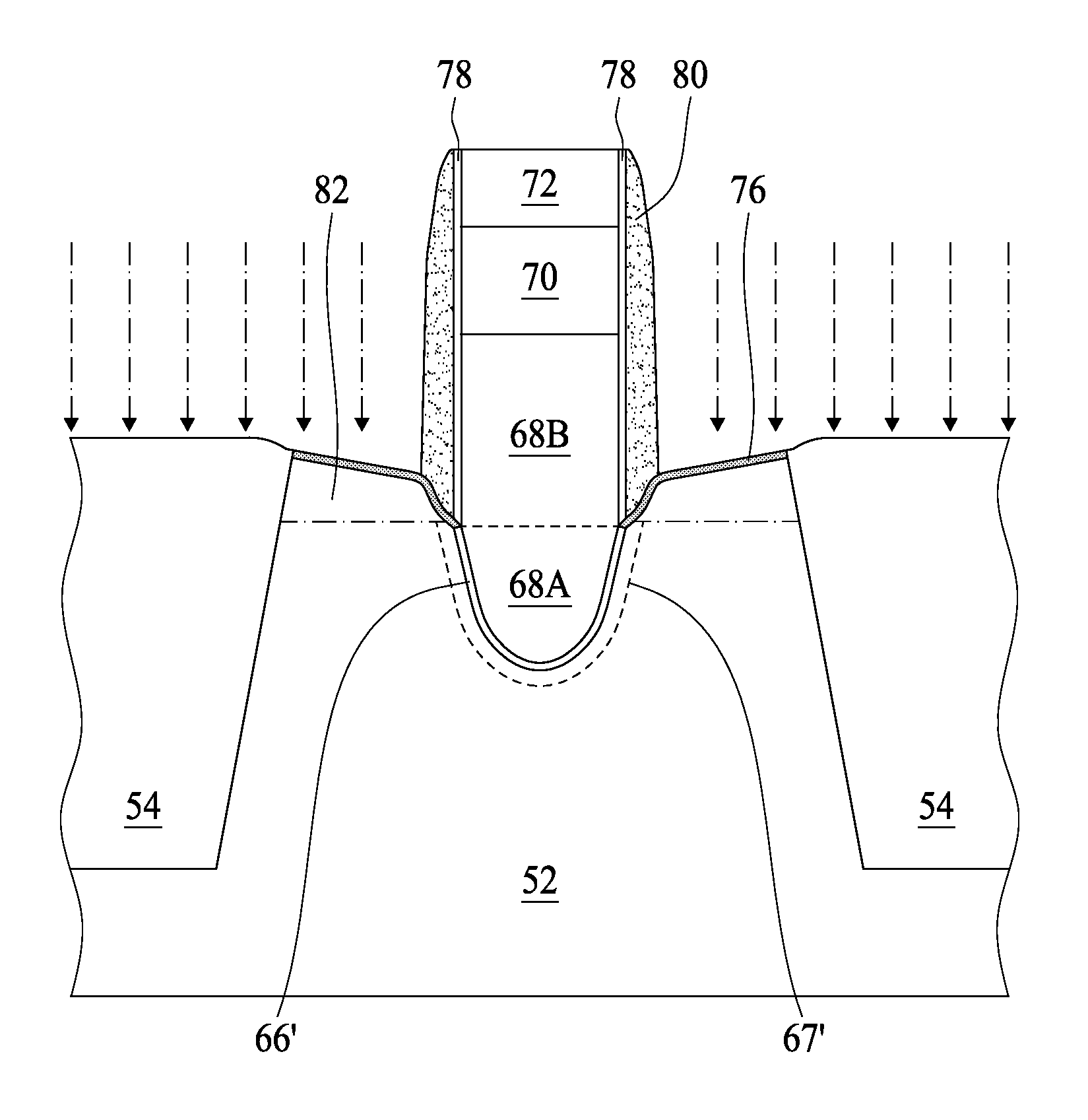
[0018]FIG. 5 to FIG. 15 illustrate a method for preparing a recessed channel transistor 50 according to one embodiment of the present invention. First, a pad oxide layer 56 is formed by the thermal oxidation process on the surface of a semiconductor substrate 52 such as a silicon substrate with a shallow trench isolation (STI) structure 54, and a pad nitride layer 58 is formed on the pad oxide layer 54 by the deposition process followed by a lithographic process and dry etching process to form an opening 58′ in the pad nitride layer 58. Subsequently, a dry etching process is performed by using the pad nitride layer 58 as an etching mask to remove a portion of the semiconductor substrate 52 under the opening 58′ of the pad nitride layer 58 to form a recess 60 in the semiconductor substrate 52.

[0019]Referring to FIG. 6, a thermal oxidation process is performed to form an oxide layer 62 on the inner sidewall of the recess 60, and an etching process is then performed to remove a corner ...


PUM


Abstract

A recessed channel transistor comprises a semiconductor substrate having a trench isolation structure, a gate structure having a lower block in the semiconductor substrate and an upper block on the semiconductor substrate, two doped regions positioned at two sides of the upper block and above the lower block, and an insulation spacer positioned at a sidewall of the upper block and having a bottom end sandwiched between the upper block and the doped regions. In particular, the two doped regions serves as the source and drain regions, respectively, and the lower block of the gate structure serves as the recessed gate of the recessed channel transistor.

Description

BACKGROUND OF THE INVENTION[0001](A) Field of the Invention[0002]The present invention relates to a recessed channel transistor and method for preparing the same, and more particularly, to a recessed channel transistor with elevated doped regions serving as source and drain regions and a method for preparing the same.[0003](B) Description of the Related Art[0004]FIG. 1 illustrates a planar channel metal-oxide-semiconductor field effect transistor (MOSFET) 10 according to the prior art. The planar channel transistor 10 is an important basic electronic device including a semiconductor substrate 12, a gate oxide layer 14, a conductive metal layer 16 serving as the gate and two doped regions 18 serving as the source / drain in the semiconductor substrate 12. The planar channel transistor 10 may further include a nitride spacer 22 positioned on the sidewall of the conductive metal layer 16 for isolating the conductive metal layer 16 from the other electronic device on the semiconductor sub...

Claims


Application Information

Patent Timeline
Patent Type & Authority Patents(United States)
IPC IPC(8): H01L29/78
CPCH01L29/1037H01L29/6659H01L29/66621H01L29/7834H01L21/28061
Inventor WU, HSIAO CHELI, MING YENTSAI, WEN LITSAI, BIN SIANG
Owner PROMOS TECH INC
Why Eureka
Try Eureka