Methods and apparatus for making integrated circuit package including opening exposing portion of the IC

a technology of integrated circuits and openings, applied in the field of electronics, can solve the problems of high cost, high volume, and inability to meet the needs of reliable methods, and achieve the effect of high reliability manufacturing and low cos

Inactive Publication Date: 2006-05-23
INTERCONNECT SYST GROUP +1
View PDF32 Cites 49 Cited by
  • Summary
  • Abstract
  • Description
  • Claims
  • Application Information

AI Technical Summary

Benefits of technology

[0009]In view of the foregoing background, it is therefore an object of the present invention to provide a method for making an IC package to have an exposed portion which is amenable to low cost, high reliability manufacturing.

Problems solved by technology

Methods for packaging IC's with an opening therein have generally been cumbersome and expensive, such as requiring specialized pre-made packaging and flexible or rigid printed circuit boards.
These approaches are not well-suited to reliable, high volume, low cost manufacturing.
Indeed, despite continuing significant developments, such as those described in the above noted Salatino et al. patent, a number of challenges are still presented for an IC package that exposes a portion of the IC.
For example, it may be difficult to keep encapsulating material from bleeding under a mold protrusion that contacts the IC to form the opening.
Preventing crush damage to the IC from foreign particles pressed between the mold and the IC also remains a challenge.

Method used


Image

  • Methods and apparatus for making integrated circuit package including opening exposing portion of the IC
  • Methods and apparatus for making integrated circuit package including opening exposing portion of the IC
  • Methods and apparatus for making integrated circuit package including opening exposing portion of the IC

Examples


Embodiment Construction

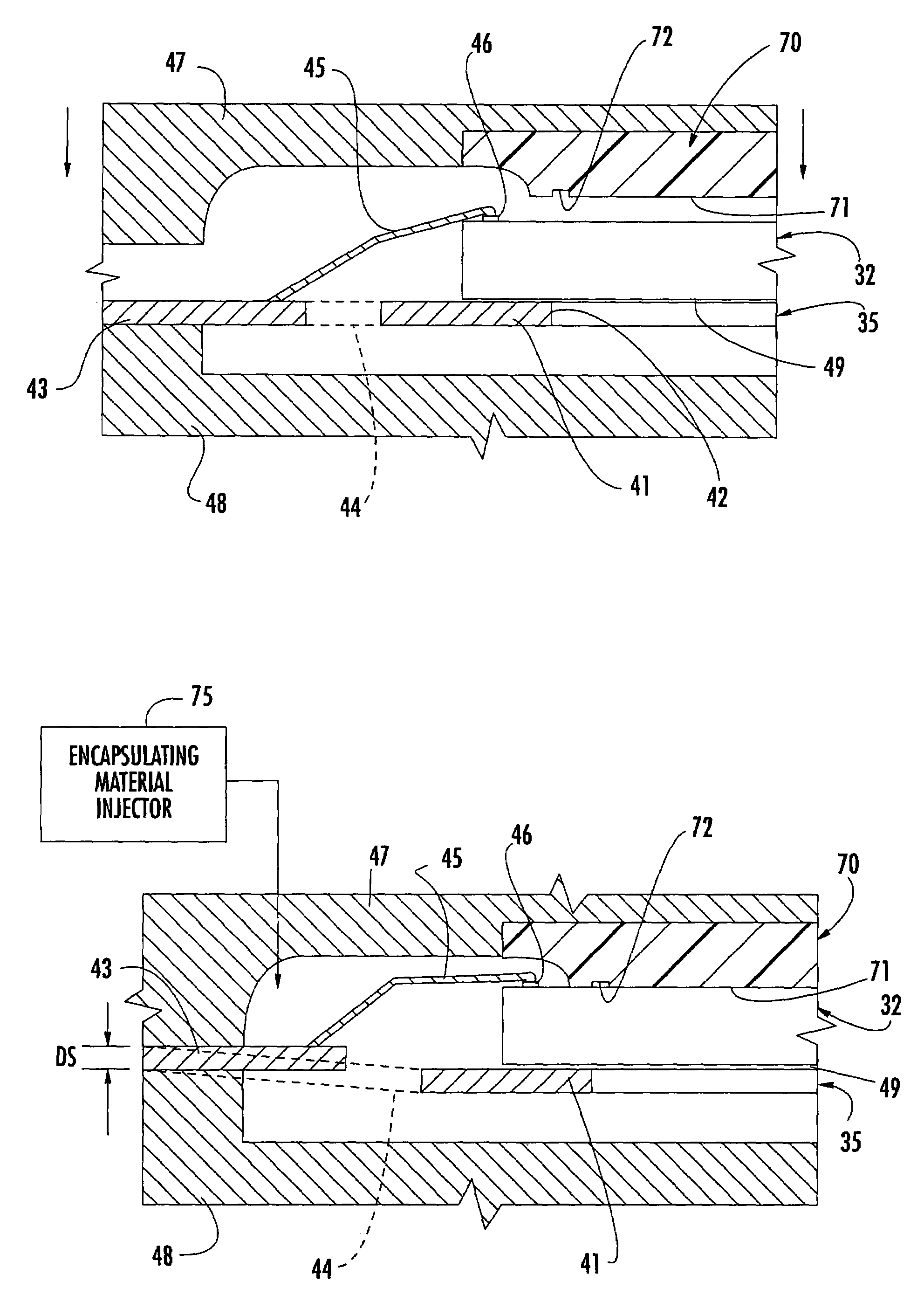
[0026]The present invention will now be described more fully hereinafter with reference to the accompanying drawings, in which preferred embodiments of the invention are shown. This invention may, however, be embodied in many different forms and should not be construed as limited to the embodiments set forth herein. Rather, these embodiments are provided so that this disclosure will be thorough and complete, and will fully convey the scope of the invention to those skilled in the art. Like numbers refer to like elements throughout.

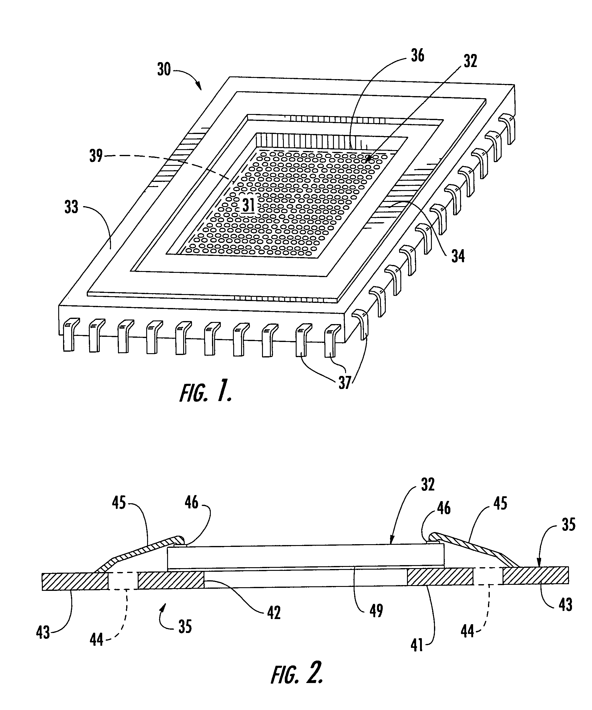
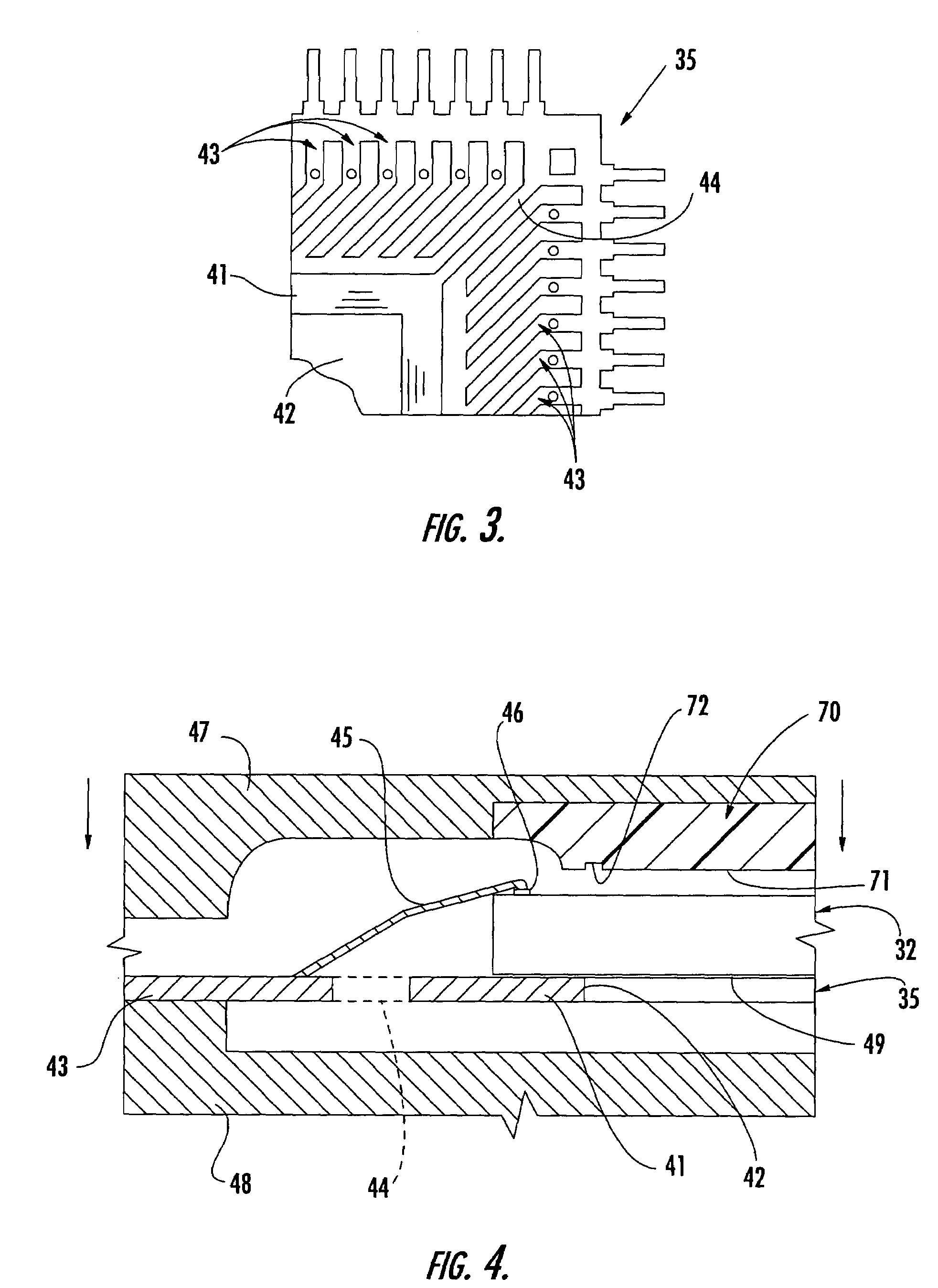
[0027]For clarity of explanation, the present invention is explained with reference to manufacturing methods for making an IC package 30 in the illustrated form of an electric field fingerprint sensor IC package as shown in FIG. 1. The electric field fingerprint sensor IC package 30 may of the type using an electric field to sense the ridges and valleys of a fingerprint as offered by AuthenTec, Inc. of Melbourne, Florida under the designation FingerLoc™ AF...


PUM

PropertyMeasurementUnit
thicknessaaaaaaaaaa
thickaaaaaaaaaa
distanceaaaaaaaaaa

Abstract

A method for making an IC package preferably includes providing a mold including first and second mold portions, and wherein the first mold portion carries a mold protrusion defining an IC-contact surface with peripheral edges and a bleed-through retention channel positioned inwardly from the peripheral edges. The method also preferably includes closing the first and second mold portions around the IC and injecting encapsulating material into the mold to encapsulate the IC and make the IC package having an exposed portion of the IC adjacent the mold protrusion. Morever, the bleed-through retention channel retains any encapsulating material bleeding beneath the peripheral edges of the IC contact surface, and prevents the encapsulating material from reaching further onto the exposed portion of the IC. The method may also include releasing the IC package with the exposed portion from the mold.

Description

RELATED APPLICATION[0001]This application is based upon U.S. provisional application Ser. No. 60 / 225,972 filed Aug. 17, 2001, the entire contents of which are incorporated herein by reference.FIELD OF THE INVENTION[0002]The present invention relates to the field of electronics, and, more particularly, to methods for making integrated circuit packages.BACKGROUND OF THE INVENTION[0003]Integrated circuit (IC) devices or packages are used in a wide variety of electronic applications including computers, cellular telephones, entertainment systems, etc. A typical IC package includes a chip of semiconductor material, or IC, in which active electronic devices are formed. Surrounding the IC is an encapsulating material, such as typically formed of a thermosetting or thermoplastic resin compound. To protect the IC from damage or contamination, the encapsulating material typically totally surrounds the IC.[0004]The IC itself may be carried by a leadframe. The leadframe includes a die pad which...

Claims


Application Information

Patent Timeline
Patent Type & Authority Patents(United States)
IPC IPC(8): H01L21/00H01L21/44H01L21/48H01L21/50G06K9/00H01L21/56H01L23/31
CPCG06K9/0002H01L21/565H01L23/3107H01L24/48H01L2924/0102H01L2224/48091H01L2924/00014H01L2224/05599H01L2224/45099H01L2224/85399H01L2924/14H01L2924/181G06V40/1306H01L2224/45015H01L2924/207H01L2924/00
Inventor SALATINO, MATTHEW M.WEBER, PATRICK O.
Owner INTERCONNECT SYST GROUP
Why Eureka
Try Eureka