Spin barrier enhanced dual magnetoresistance effect element and magnetic memory using the same

a dual magnetoresistance and effect element technology, applied in the field of magnetic memory systems, can solve the problems of large transistor size and high power consumption, and achieve the effects of reducing the contribution of the outer surface, eliminating the damping of spin pumping, and high areal resistan

Active Publication Date: 2006-06-06
SAMSUNG SEMICON
View PDF6 Cites 214 Cited by
  • Summary
  • Abstract
  • Description
  • Claims
  • Application Information

AI Technical Summary

Benefits of technology

[0033]The present invention provides a method and system for providing a magnetic element that can be used in a magnetic memory. The magnetic element includes first pinned, spacer, free, spin barrier, and second pinned layers. The spacer layer is nonmagnetic and resides between the pinned and free layers. The free layer can be switched using spin transfer when a write current is passed through the magnetic element. The free layer resides between the spacer layer and the spin barrier layer. The spin barrier layer is between the free layer and the second pinned layer. The spin barrier layer is configured to reduce an outer surface contribution to a damping constant of the free layer. In one aspect, the spin barrier layer has a high areal resistance and may substantially eliminate spin pumping induced damping. In another aspect, the magnetic element also includes a spin accumulation layer between the spin barrier and free layers. The spin accumulation layer is metallic and may have a long spin diffusion length.
[0034]According to the system and method disclosed herein, the present invention provides a magnetic element that can be switched due to spin transfer using a lower current density and the attendant advantages of a lower switching current density.

Problems solved by technology

The high operating current leads to design problems for high density MRAM, such as heating, high power consumption, large transistor size, as well as other issues.

Method used


Image

  • Spin barrier enhanced dual magnetoresistance effect element and magnetic memory using the same
  • Spin barrier enhanced dual magnetoresistance effect element and magnetic memory using the same
  • Spin barrier enhanced dual magnetoresistance effect element and magnetic memory using the same

Examples


first embodiment

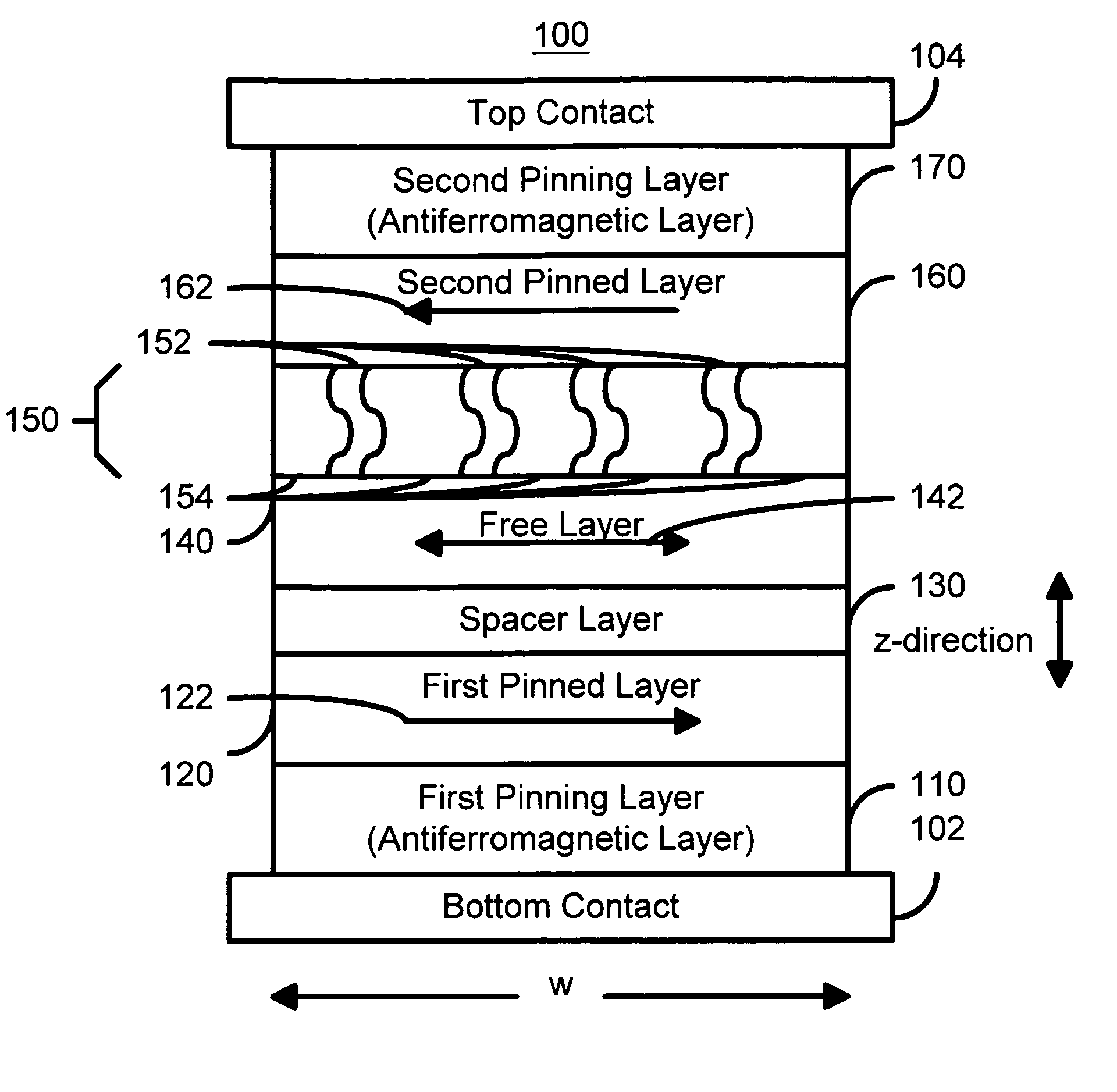
[0049]To more particularly illustrate the method and system in accordance with the present invention, refer now to FIG. 3A, depicting a portion of a magnetic element 100 in accordance with the present invention having a reduced write current density for spin transfer switching. The magnetic element 100 is preferably used in a magnetic memory, such as a MRAM, in a CPP configuration. Thus, the magnetic element 100 may be used in a memory cell including an isolation transistor (not shown), as well as other configurations of magnetic memories. Moreover, the magnetic element 100 preferably utilizes the two terminals 102 and 104 near the top and bottom, respectively, of the magnetic element 100. However, nothing prevents the use of another number of terminals, for example a third terminal near the center of the magnetic element. The magnetic element 100 includes a first pinned layer 120, a spacer layer 130, a free layer 140, and a second pinned layer 160. The magnetic element 100 generall...

second embodiment

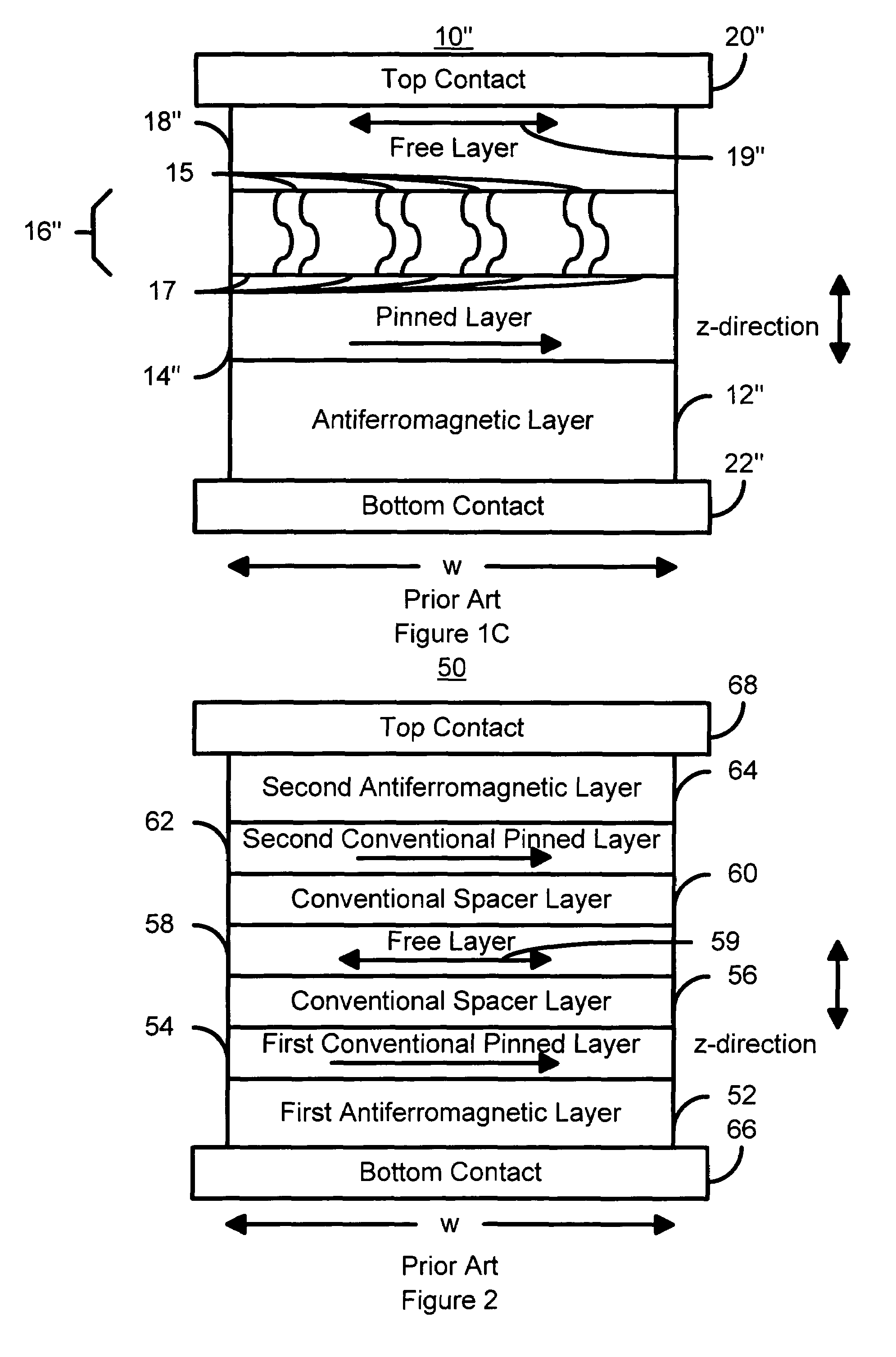
[0070]FIG. 4A depicts a portion of a magnetic element 200 in accordance with the present invention having a reduced write current density for spin transfer. The magnetic element 200 is preferably used in a magnetic memory, such as a MRAM, in a CPP configuration. Thus, the magnetic element 200 may be used in a memory cell including an isolation transistor (not shown), as well as other configurations of magnetic memories. Moreover, the magnetic element 200 preferably utilizes the two terminals 202 and 204 near the top and bottom, respectively, of the magnetic element 200. However, nothing prevents the use of another number of terminals, for example a third terminal near the center of the magnetic element. The magnetic element 200 includes a first pinned layer 220, a spacer layer 230, a free layer 240, a spin accumulation layer 250, a spin barrier layer 260, and a second pinned layer 270. The magnetic element 200 generally also includes a first pinning layer 210 used to pin the magneti...


PUM


Abstract

A method and system for providing a magnetic element that can be used in a magnetic memory is disclosed. The magnetic element includes first pinned, spacer, free, spin barrier, and second pinned layers. The spacer layer is nonmagnetic and resides between the pinned and free layers. The free layer can be switched using spin transfer when a write current is passed through the magnetic element. The free layer resides between the spacer and spin barrier layers. The spin barrier layer is between the free and second pinned layers. The spin barrier layer is configured to reduce an outer surface contribution to the free layer damping constant. In one aspect, the spin barrier layer has a high areal resistance and may substantially eliminate spin pumping induced damping. In another aspect, the magnetic element also includes a spin accumulation layer between the spin barrier and free layers. The spin accumulation layer has a high conductivity and may have a long spin diffusion length.

Description

FIELD OF THE INVENTION[0001]The present invention relates to magnetic memory systems, and more particularly to a method and system for providing a magnetic element that employs a spin transfer effect in switching and that can be switched using a lower switching current density.BACKGROUND OF THE INVENTION[0002]FIGS. 1A, 1B, and 1C depict conventional magnetic elements 10, 10′, and 10″ that can be used in magnetic memories. Note that recent reviews of developments in the field of magnetic memories can be found for example in: “Memories of Tomorrow”, by William Reohr et al., IEEE Circuits and Devices Magazine, pp. 17–27, September 2002; and “Magnetoresistive Random Access Memory Using Magnetic Tunnel Junctions”, by Saied Tehrani et al., Proceedings of the IEEE, vol. 91, no. 5, pp. 703–714, May 2003. The conventional magnetic element 10 is a spin valve and includes a conventional antiferromagnetic (AFM) layer 12, a conventional pinned layer 14, a conventional spacer layer 16 that is con...

Claims


Application Information

Patent Timeline
Patent Type & Authority Patents(United States)
IPC IPC(8): G11C11/00G11C11/16
CPCH01L43/08G11C11/16H10N50/10B82Y25/00G11C11/15G11C11/161H10B61/00H10N50/85
Inventor VALET, THIERRY
Owner SAMSUNG SEMICON
Why Eureka
Try Eureka