

Method of fabricating thin film transistor TFT array
a thin film transistor and array technology, applied in transistors, electrical devices, semiconductor devices, etc., can solve the problems of high-diffusion wiring exposure times in the masking process and and achieve the effect of reducing high-diffusion wiring exposure times and reducing component defects in metal wiring
- Summary
- Abstract
- Description
- Claims
- Application Information
AI Technical Summary
Benefits of technology
Problems solved by technology
Method used
Image

Examples
Embodiment Construction
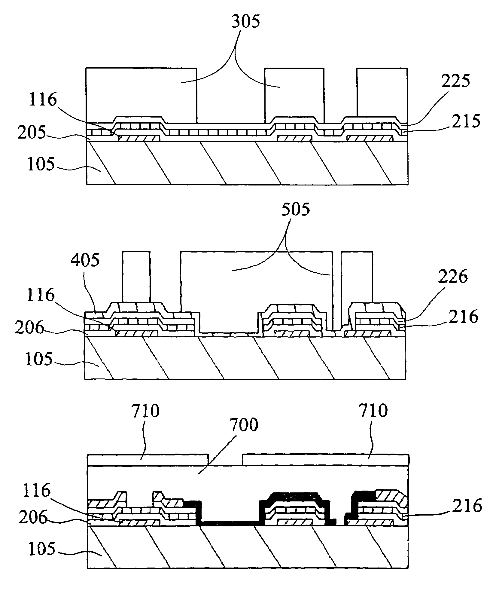
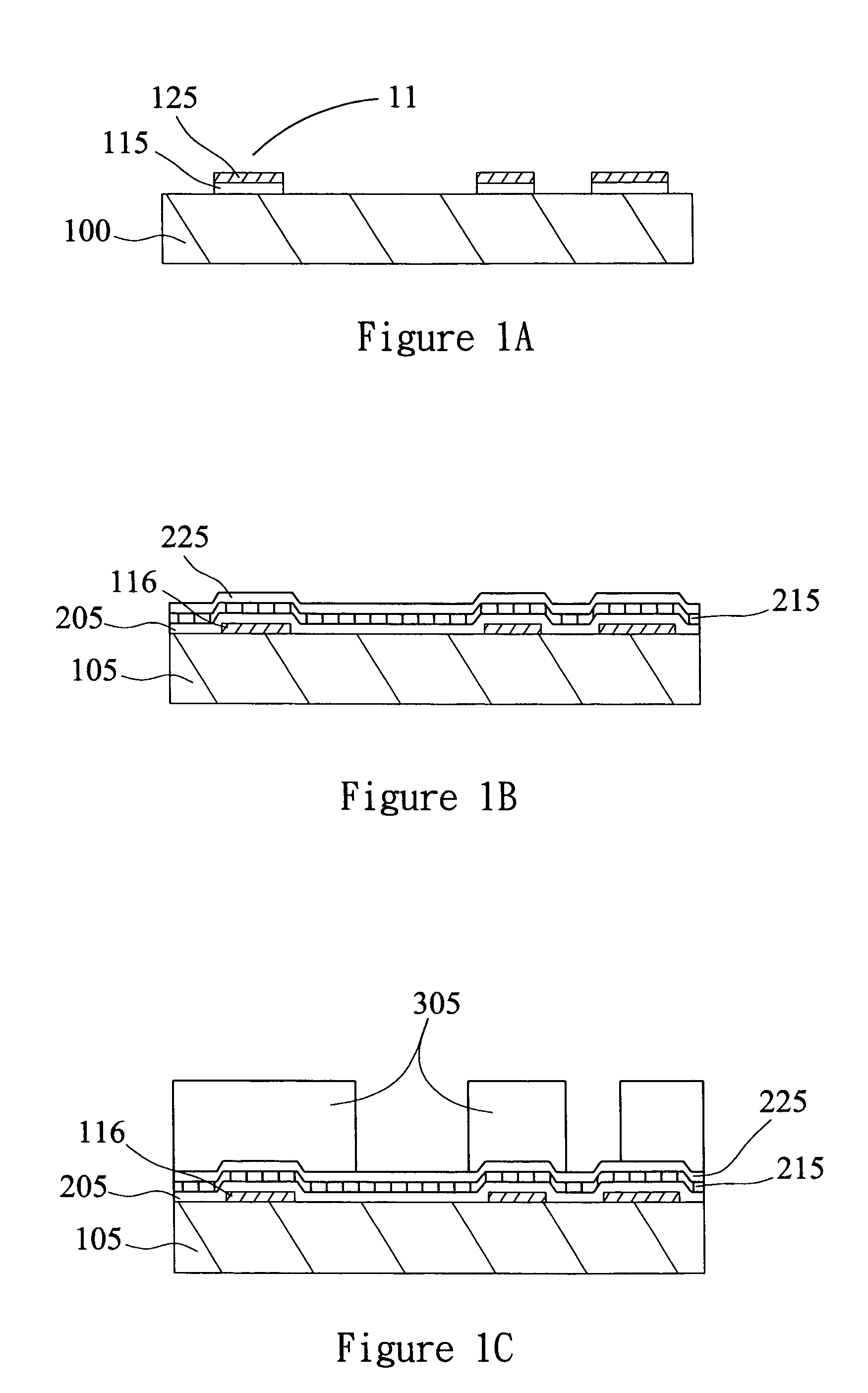
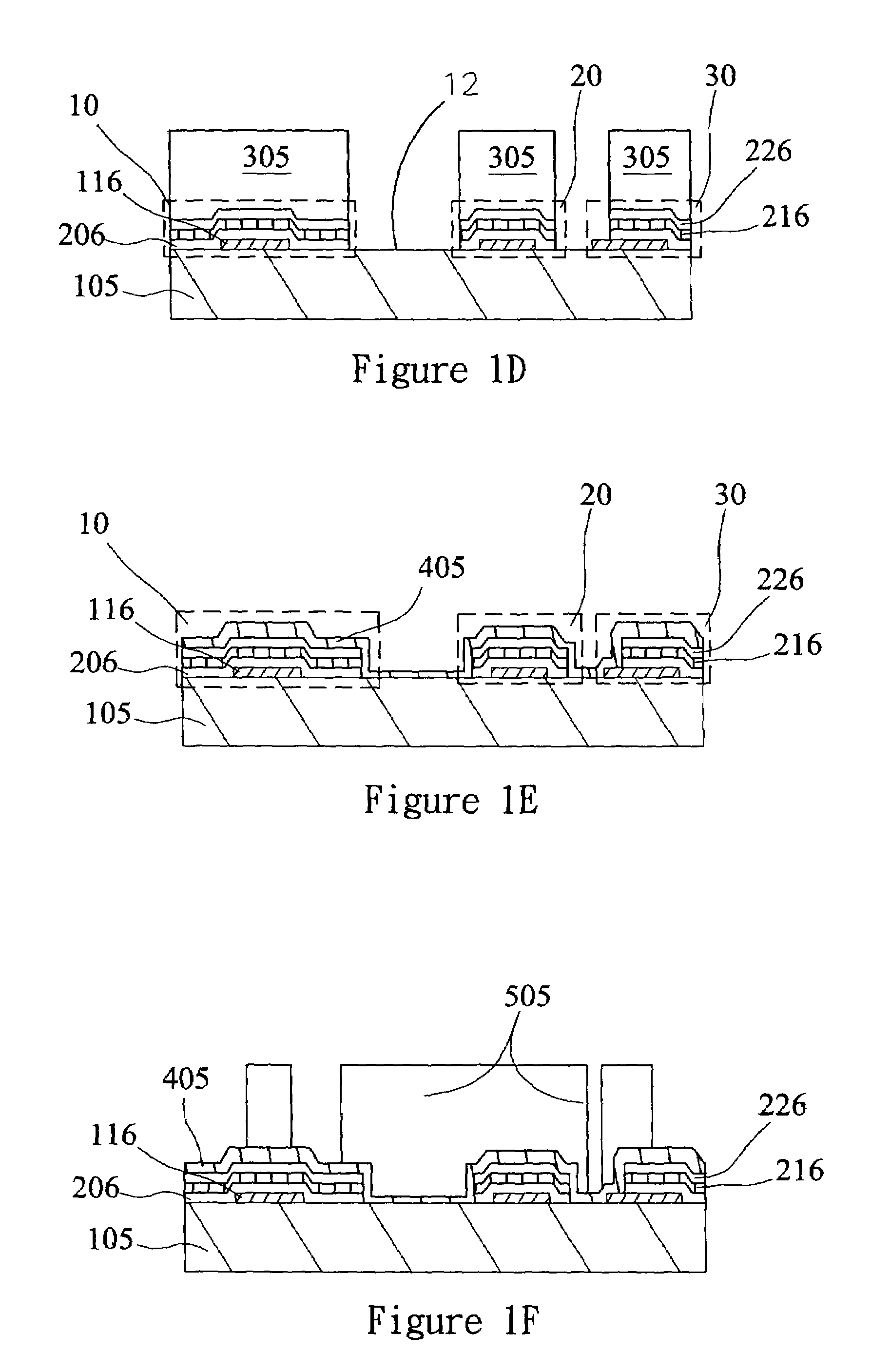
[0010]FIG. 1A illustrates step 1 of one of the preferred embodiments according to the present invention, in which a mask is used to define the position of the gate electrode metal wiring on the substrate 100. Then, α-Si seed layer 115 is formed on the position. Then, the desired-plated metal 125 and the graphs of the desired-plated area which being are made by relatively strong oxidation-reduction materials processes of ion replacement to form the gate electrode 11. The ion of the desired metal can be Cu, Al, Ag, In, Ti, W, and MO. The desired-plated graph made from the stronger reduction materials can be an α-Si seed layer 15. Then, as shown in FIG. 1B, the deposition of the dielectric layer 205 on the resulting ion-replaced seed layer 116 is carried out, followed by deposition of α-Si layer 215, and N+ Si layer 225. FIG. 1B, shows step two of the preferred embodiment illustrated in FIG. 1. The α-Si layer can be used as a conducting channel, while the N+ Si layer can be used as an ...
PUM
 Abstract
Description
Claims
Application Information