Method of inspecting curved surface and device for inspecting printed circuit board

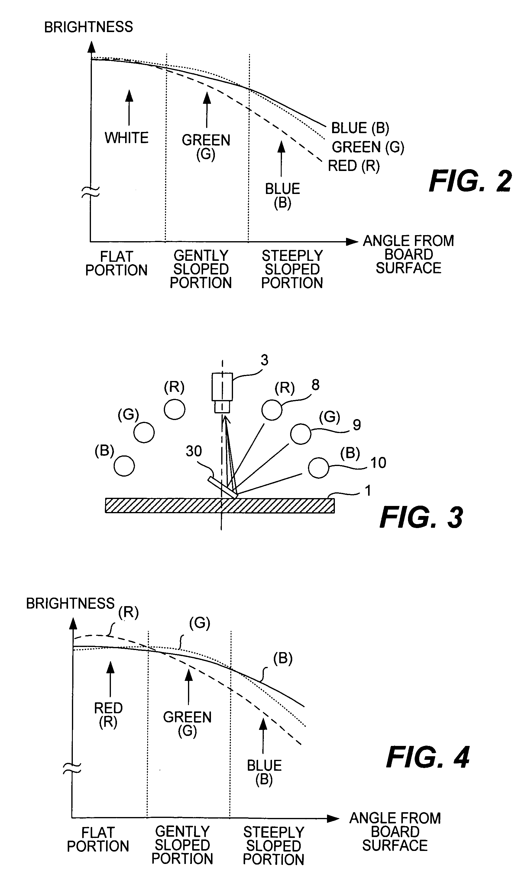
a technology of printed circuit board and curved surface, which is applied in the direction of color/spectral properties measurement, instruments, material analysis, etc., can solve the problems of difficult visual recognition of red color on the flat solder surface portion close to the disposed diffusive reflecting plate, and long time to visually determine the appropriate threshold value. , to achieve the effect of clearer color distribution

Inactive Publication Date: 2006-06-13
ORMON CORP
View PDF16 Cites 9 Cited by
  • Summary
  • Abstract
  • Description
  • Claims
  • Application Information

AI Technical Summary

Benefits of technology

[0008]It is therefore an object of this invention to carry out a reliable inspection even on a curved surface of a target object having a high diffusive reflectivity such as lead-free solder.
[0020]By this method, each image of a sloped surface corresponding to the direction of a light source is adjusted such that the color component which would be dominant if the sloped surface were a mirror surface will be emphasized. Thus, even if the curved surface of the target object has a high diffusive reflectivitly and the differences in brightness among the color components are difficult to observe, the a color distribution according to the sloping angle can be obtained. Since the whiteness-extracting, brightness-reducing and brightness restoring processes are carried out thereafter, the effects of diffusive reflected light can be eliminated and images with a clear color distribution can be obtained.
[0026]With the methods described above, even the conditions of a diffusively reflecting surface can be automatically inspected with a high accuracy. When the condition of a curved surface is inspected visually by an operator, the inspection method may include the steps of displaying the image after the brightness-restoring process and receiving the data item indicating the operator's judgment. By such a displaying step, the operator can clearly see the distribution conditions of the color components at different sloping angles and hence an accurate judgment can be rendered.
[0035]With the inspection device of this invention, the processes by the whiteness-removing and brightness-restoring means are carried out also on the image picked up at the time of teaching and inputted and the processed image is displayed on the display device. Thus, the operator can easily select a position on the displayed image suited for the binary threshold value and the judgment reference value, and the processes of setting data for the inspection and registering them can be carried out efficiently.
[0037]Since the image of the solder to be inspected after the whiteness-removing and brightness-restoring processes can be displayed on the display device, an accurate visual inspection is possible based on the color distribution made clearer according to the slope of the solder surface.
[0040]With such brightness-adjusting means, the image of the solder to be inspected is adjusted before the whiteness-extracting and brightness-restoring processes such that the color component corresponding to the sloping angle of the solder surface is emphasized. When the surface of lead-free solder with diffusive reflectivity is inspected, a color distribution according to the slope of the surface is obtained and then the effects of diffusively reflected light are removed such that the color distribution can be made clearer.

Problems solved by technology

Thus, if an image is formed of an object with a high diffusive reflectivity such as lead-free solder, the image as a whole becomes white as each color component is mixed together or the boundaries between color patterns become unclear and obscure.
Thus, the red color on the flat solder surface portion close to the disposed diffusive reflecting plate becomes particularly difficult to recognize visually.
If a whitish image is generated because the color components are mixed together or if the boundaries between the color patterns become unclear, however, it is not easy and may take a long time to visually determine an appropriate threshold value for binary conversion.
This optical system may be used for a visual inspection device, but it takes a long time to evaluate the condition of each target area to be inspected if it becomes difficult to ascertain subtle color differences at boundary areas between different color patterns.
If the diffusive reflectivity of the lead-free solder to be inspected increases, furthermore, the difference in brightness gradation of the color components becomes smaller, making it difficult to maintain a high level of accuracy in the inspection.

Method used


Image

  • Method of inspecting curved surface and device for inspecting printed circuit board
  • Method of inspecting curved surface and device for inspecting printed circuit board
  • Method of inspecting curved surface and device for inspecting printed circuit board

Examples


Embodiment Construction

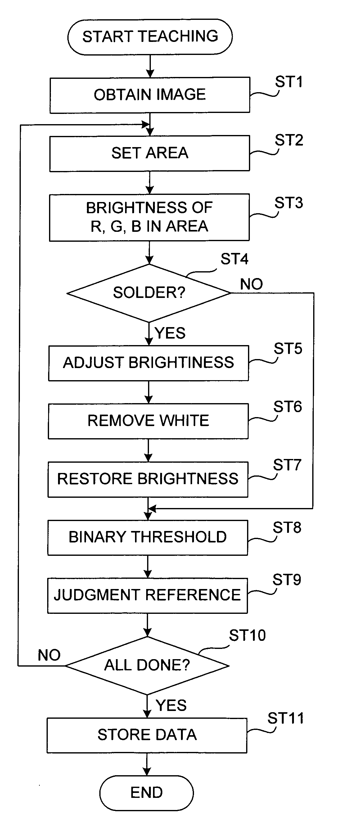
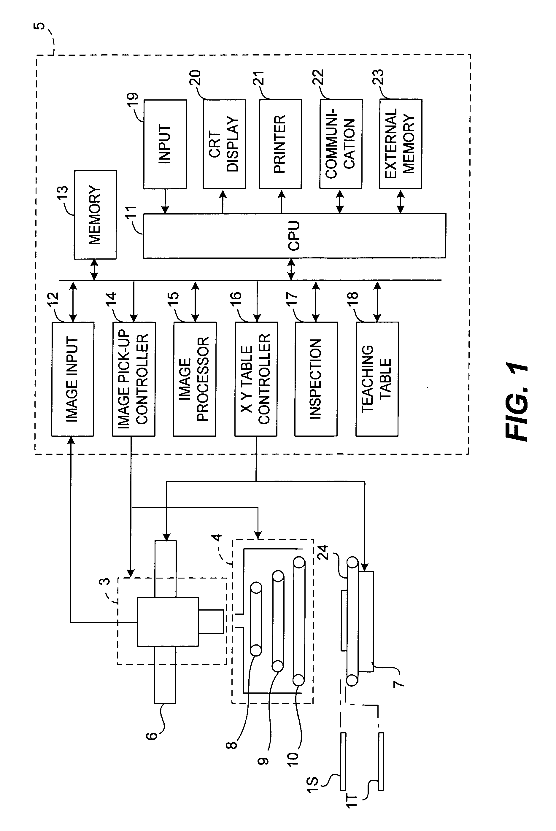
[0052]The invention is described next by way of an example of a device for inspecting a printed circuit board with lead-free solder by obtaining an image of the circuit board and to process the image thus obtained, thereby determining the quality of soldered parts thereon. As shown in FIG. 1, the device comprises an image pick-up device 3, a light projecting device 4, a control unit 5, an X-table 6 and a Y-table 7. In FIG. 1, the target circuit board to be inspected is indicated by symbol 1T and a standard printed circuit board with properly soldered parts indicated by symbol 1S.

[0053]The Y-table 7 is provided with a conveyer 24 for supporting the circuit board 1S or 1T and adapted to be moved by a motor (not shown) to transport the circuit board 1S or 1T in the Y-direction (perpendicular to the plane of the page). The X-table 6 supports the image pick-up device 3 and the light projecting device 4 to move them in the X-direction (the left-right direction on the page) above the Y-tab...


PUM

PropertyMeasurementUnit
angleaaaaaaaaaa
angleaaaaaaaaaa
surface conditionsaaaaaaaaaa

Abstract

A circuit board with lead-free solder is inspected by using light sources with different colors at different angles to obtain an image having a plurality of color components. For each pixel within an area in the obtained image, the brightness of a white component generated by mixing all of the color components is extracted. The brightness of each of the color components of each pixel is reduced by an amount corresponding to the extracted brightness of the white component and is adjusted such that the brightest of the color components becomes more strongly emphasized compared to the others, than the brightness before the brightness-reducing process was carried out and the loss in total brightness caused by the brightness-reducing process is restored. The image with restored brightness is displayed and the surface condition of the solder is judged on the basis of the distributions of the color components of this image.

Description

BACKGROUND OF THE INVENTION[0001]This invention is in the technical field of inspecting a curved surface of an object such as a soldered part on a printed circuit board.[0002]Japanese Patent Publication Tokko 6-1173 describes a device for automatically inspecting a soldered part on a printed circuit board by a method of image processing by making use of the mirror reflection from the solder part. As shown in FIG. 9, this device serves to form an image of a target object to be inspected by means of three light sources 8, 9 and 10 emitting respectively red (R), green (G) and blue (B) light and an image pick-up device 3. Each of the light sources 8, 9 and 10 is disposed obliquely above the solder 2 to be inspected. With a device thus structured, each of the colored light beams from the sources8, 9 and 10 makes incidence on the solder 2 at a different position corresponding to the angular orientation of its source. If the solder surface is sloped so as to be able to lead the mirror-refl...

Claims


Application Information

Patent Timeline
Patent Type & Authority Patents(United States)
IPC IPC(8): G06K9/00G01N21/27G01N21/956G01R31/309
CPCG01N21/274G01N21/95684G01R31/309G01N2021/95646G01N2021/95638
Inventor OSHIUMI, AKIRAFUJII, YOSHIKIFUJITA, YUJIN
Owner ORMON CORP
Why Eureka
Try Eureka