Multi-layer printed circuit board fabrication system and method

Inactive Publication Date: 2006-06-13
ORBOTECH LTD
View PDF13 Cites 19 Cited by
  • Summary
  • Abstract
  • Description
  • Claims
  • Application Information

AI Technical Summary

Problems solved by technology

Among the problems which arise in printed circuit board fabrication is the side to side alignment of printed circuit patterns on various substrate layers, and mutual alignment among patterns printed on various substrate layers.

Method used


Image

  • Multi-layer printed circuit board fabrication system and method
  • Multi-layer printed circuit board fabrication system and method
  • Multi-layer printed circuit board fabrication system and method

Examples


embodiment 200

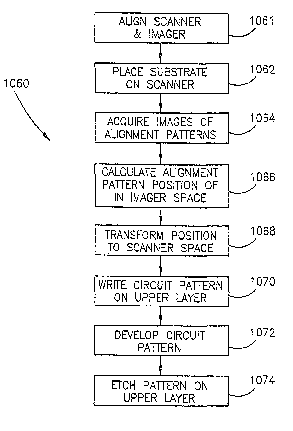
[0074]FIGS. 3 and 4 show an embodiment 200 of the present invention, which includes apparatus enabling the use of a new method of determining the relative position of the printed circuit board in the scanner useful for aligning images to be written on the respective opposing sides of a printed circuit board.

[0075]In this system, a principal difference from the prior art system of FIGS. 1 and 2 resides in the mechanism for determining a reference for the scanner for writing an electrical circuit pattern.

Scanner—Imager Coordinate Calibration

[0076]It is appreciated that in order to align patterns that are sequentially recorded on a substrate a mechanism is required to coordinate between the respective location of the subsequently recorded patterns. In exemplary embodiments of the invention, an acquired image of a reference pattern is employed. It is desirable to tie together the location of the reference pattern in images to coordinate space of the scanner system to ensure that recorde...

first embodiment

[0154]The invention has been described utilizing exemplary apparatus and exemplary methods. It should be understood that other apparatus may be used in carrying out the methods and the methods described may be useful in apparatus that is different from that described. For example, conventional projection exposure systems may be used to record patterns. Furthermore, since each of the methods is, in great measure, a stand alone method, other methods may be utilized in determining one or more of the calibrations described. In particular, it may be possible, under certain circumstances, to delete or simplify one of the calibrations, as for example when the devices are produced to a very high tolerance or where very high accuracy is not needed. In addition, while a system using two imagers has been described, a single imager may be used in one of two ways. In a first embodiment, the imager has a large enough field of view to encompass multiple patterns on the substrate. Generally, this e...


PUM

PropertyMeasurementUnit
electricalaaaaaaaaaa
electrical circuitaaaaaaaaaa
transparentaaaaaaaaaa

Abstract

A method for aligning an image to be recorded by a direct image scanner on an upper layer of a printed circuit board with an image recorded on a lower layer thereof, the method comprising visually imaging a portion of the image on the lower layer and recording a pattern on the upper layer, referenced to coordinates of the visual image of the portion.

Description

[0001]This application is a §371 National Stage Entry of PCT / IL01 / 01027 filed on Nov. 6, 2001; PCT / IL01 / 01027 is a continuation in part of U.S. application Ser. No. 09 / 708,160 filed Nov. 8, 2000 (now U.S. Pat. No. 6,819,789); PCT / IL01 / 01027 is a continuation of U.S. application Ser. No. 09 / 792,498 filed Feb. 23, 2001 (now U.S. Pat. No. 6,701,197); PCT / IL01 / 01027 claims priority also from Israel Application 142354 filed Apr. 1, 2001.FIELD OF THE INVENTION[0002]The present invention is related to the field of electrical circuit fabrication and especially to the field of printed circuit board fabrication employing a laser direct imaging device.BACKGROUND OF THE INVENTION[0003]It is known to manufacture printed circuit boards by way of a so-called sequentially build up methodology in which at least one outer layer is sequentially added to an already existing printed circuit board core.[0004]Systems for recording electrical circuit patterns on printed circuit board substrates include exp...

Claims


Application Information

Patent Timeline
Patent Type & Authority Patents(United States)
IPC IPC(8): G06F19/00G03F7/20G03F9/00H05K1/02H05K3/00H05K3/46
CPCG03F7/2053G03F9/00H05K3/4679H05K1/0269H05K3/0008H05K2201/09918H05K3/0082H05K3/4652H05K2201/09063H05K3/0035
Inventor GANOT, AMNOTGINO, HANANHANINA, GOLANKANTOR, ZEEVKLING, BORISSPINZI, SHABTAYBEN-EZRA, BARRY
Owner ORBOTECH LTD
Why Eureka
Try Eureka