Organic electroluminescent display device and method of fabricating the same

a technology of organic electroluminescent display and oeld, which is applied in the direction of static indicating devices, semiconductor/solid-state device details, instruments, etc., can solve the problems of limited production yield of organic el layers, limited display size and high power consumption of passive matrix oeld devices. achieve uniform image quality and uniform image quality

Active Publication Date: 2006-06-20
LG DISPLAY CO LTD
View PDF1 Cites 16 Cited by
  • Summary
  • Abstract
  • Description
  • Claims
  • Application Information

AI Technical Summary

Benefits of technology

[0019]Another object of the present invention is to provide an OELD device having uniform image quality.
[0020]Another object of the present invention is to provide a method of fabricating an OELD device having uniform image quality.

Problems solved by technology

Although the passive matrix OELD devices have simple structures and are formed by simple fabrication processes, passive matrix OELD devices require a relatively high amount of power to operate.
In addition, the display size of passive matrix OELD devices is limited due to their structure.
Since the organic EL layer's yield is relatively low, the production yield of the OELD device is limited by the organic EL layer's yield.
For example, even when a TFT is properly fabricated, an OELD device can be determined to be unacceptable due to defects of the organic EL layer using a thin film of about 1000 Å thickness.
Accordingly, this limitation causes loss of materials and an increase in production costs.
However, the bottom emission-type OELD devices are not adequate for implementation in display devices that require high resolution due to the limitations of the increased aperture ratio.
However, since a cathode is commonly formed over the organic EL layer in the top emission-type OELD devices, material selection and light transmittance are limited such that light transmission efficiency is lowered.
If a thin film type passivation layer is formed to prevent a reduction of the light transmittance, the thin film type passivation layer may fail to prevent infiltration of exterior air into the device.

Method used


Image

  • Organic electroluminescent display device and method of fabricating the same
  • Organic electroluminescent display device and method of fabricating the same
  • Organic electroluminescent display device and method of fabricating the same

Examples


Embodiment Construction

[0036]Reference will now be made in detail to the preferred embodiments of the present invention, examples of which are illustrated in the accompanying drawings.

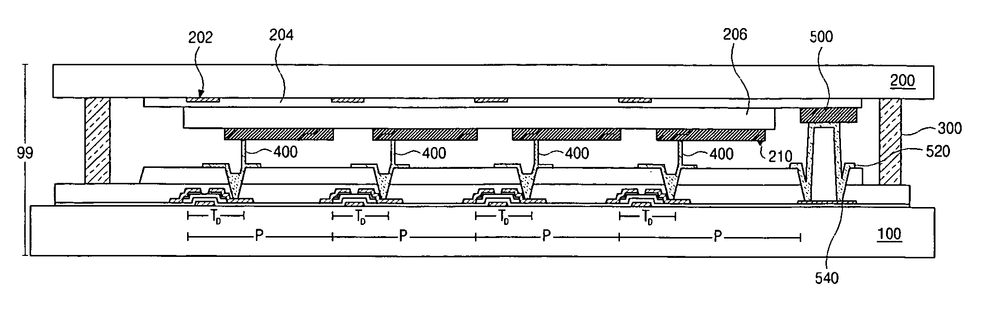
[0037]FIG. 5 is a schematic cross sectional view of an exemplary dual-plate OELD device according to the present invention. In FIG. 5, an OELD device 99 may include a first substrate 100 and a second substrate 200 spaced apart from and attached to the first substrate 100 using a sealant 300. Although not shown, an array element layer and an organic electroluminescent diode may be formed on the first and second substrates 100 and 200, respectively, and a display region and a periphery region surrounding the display region may be defined in the first and second substrates 100 and 200.

[0038]In FIG. 5, a plurality of pixel regions P may be provided within the display region, and a switching TFT (not shown) and a driving TFT TD may be formed on an inner surface of the first substrate 100 in each of the pixel regions P. Although n...


PUM


Abstract

An organic electroluminescent device includes first and second substrates spaced apart from and attached to each other, the first and second substrates including a plurality of pixel regions and a periphery region surrounding the plurality of pixel regions, a plurality of gate lines on an inner surface of the first substrate, a plurality of data lines crossing the plurality of gate lines, a plurality of driving thin film transistors, each of the driving thin film transistors adjacent to one of the plurality of pixel regions, a plurality of power lines connected to the driving thin film transistors, a plurality of gate pads connected to an end portion of the gate lines within the periphery region, a plurality of data pads connected to an end portion of the data lines within the periphery region, a plurality of power pads connected to an end portion of the power lines within the periphery region, at least one dummy pad within the periphery region, the at least one dummy pad being independent of each of the gate pads, the data pads, and the power pads, a first electrode on an inner surface of the second substrate, the first electrode connected to the dummy pad, an organic electroluminescent layer on the first electrode, a plurality of second electrodes on the organic electroluminescent layer within each of the pixel regions, and a plurality of connection electrodes electrically interconnecting the first substrate with the second substrate.

Description

[0001]The present invention claims the benefit of Korean Patent Application No. 2003-0100675, filed in Korea on Dec. 30, 2003, which is hereby incorporated by reference.BACKGROUND OF THE INVENTION[0002]1. Field of the Invention[0003]The present invention relates to an organic electroluminescent display (OELD) device and a method of fabricating an OELD device, and more particularly, to a dual-plate OELD device and a method of fabricating a dual plate OELD device.[0004]2. Discussion of the Related Art[0005]In general, an OELD device emits light by injecting electrons from a cathode and injecting holes from an anode into an emission layer, combining the electrons with the holes, generating an exciton, and transitioning the exciton from an excited state to a ground state. Unlike liquid crystal display (LCD) devices, an additional light source is not necessary for an OELD device to emit light since the transition of the exciton between the excited and ground states causes light to be emi...

Claims


Application Information

Patent Timeline
Patent Type & Authority Patents(United States)
IPC IPC(8): H01L29/04G09G3/30H05B33/06H01L23/04H01L27/32H01L51/52H05B33/02H05B33/04H05B33/10H05B33/12H05B33/26H05B44/00
CPCH01L51/5212H01L27/3276H01L27/3253H01L27/3223H10K59/88H10K59/1275H10K59/131H10K59/80516H05B33/06H10K50/814
Inventor PARK, JAE-YONG
Owner LG DISPLAY CO LTD
Why Eureka
Try Eureka