

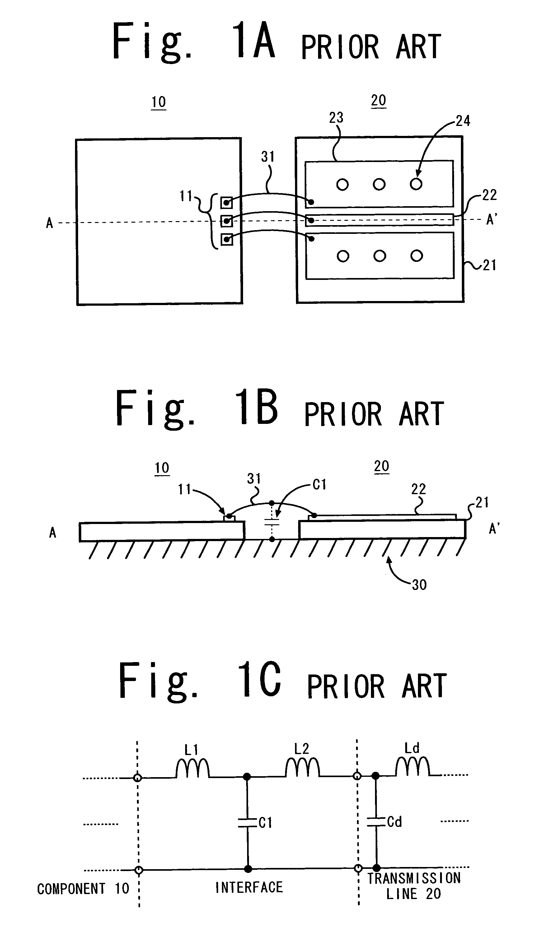
Transmission line and device including the same
a technology of transmission line and transmission line, applied in the field of transmission line, to achieve the effect of reducing the discontinuity caused between a component and the transmission lin
- Summary
- Abstract
- Description
- Claims
- Application Information
AI Technical Summary
Benefits of technology
Problems solved by technology
Method used
Image

Examples
first embodiment
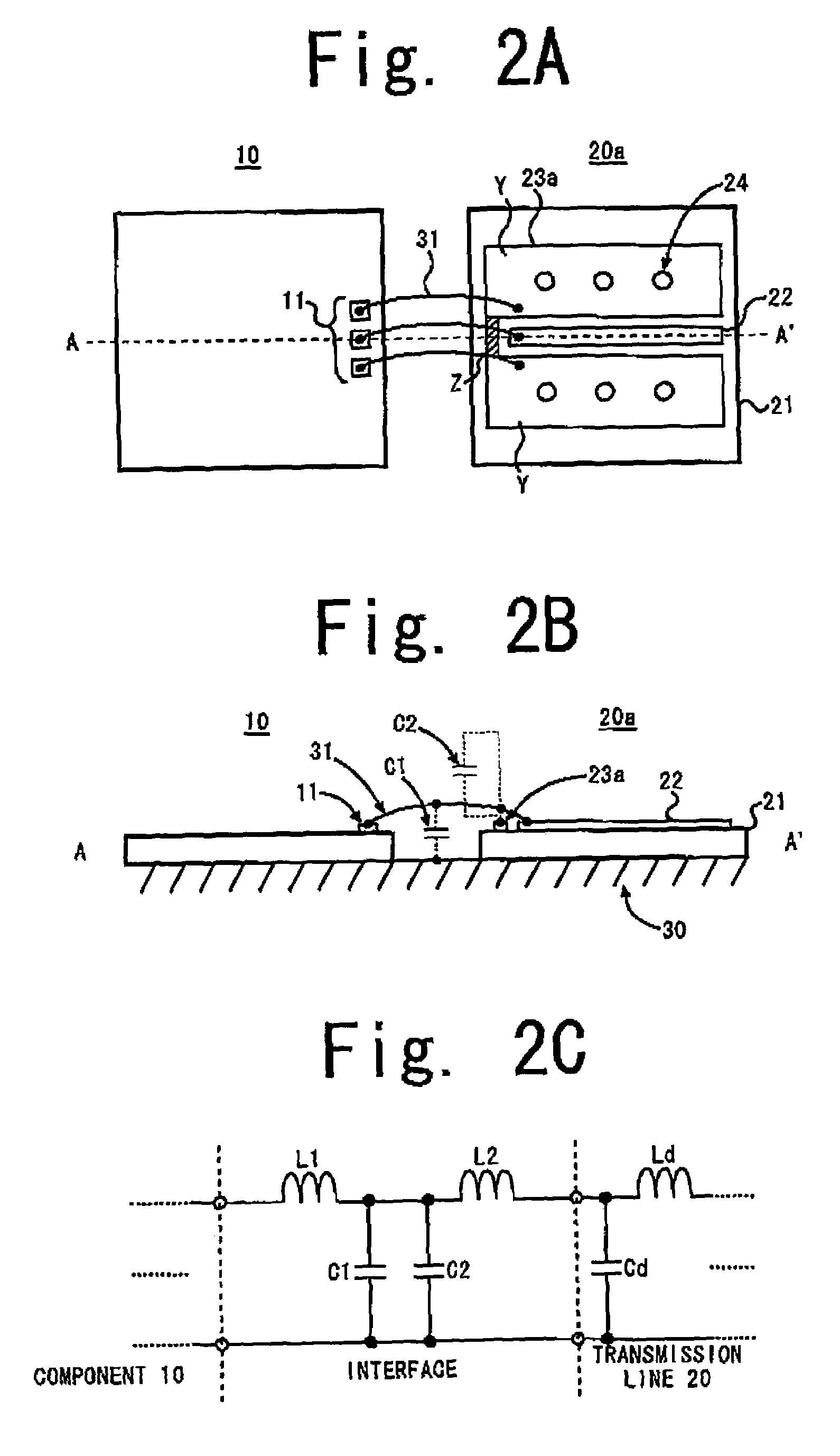
[0030]A first embodiment of the present invention employs a coplanar type transmission line.
[0031]FIG. 2A is a plan view of a device with a transmission line 20a according to the first embodiment of the present invention, in which parts that are the same as those shown in FIGS. 1A through 1C are given the same reference numerals. The component 10 and the transmission line 20a are disposed a predetermined distance apart. A signal line 22 and a ground pattern 23a of the transmission line 20a are connected to the pads 11 of the component 10 through metal wires 31 made of, for example, gold. The distance between the component 10 and the transmission line 20a depends on a design condition of the device. In this respect, it is possible to decrease the inductance of the metal wires 31 by setting the distance between the component 10 and the transmission line 20a as short as possible. By such an arrangement, it is possible to alleviate design demands of the metal wiring and the transmission...
third embodiment
[0044]A device according to a third embodiment of the invention employs a microstrip line as the transmission line.
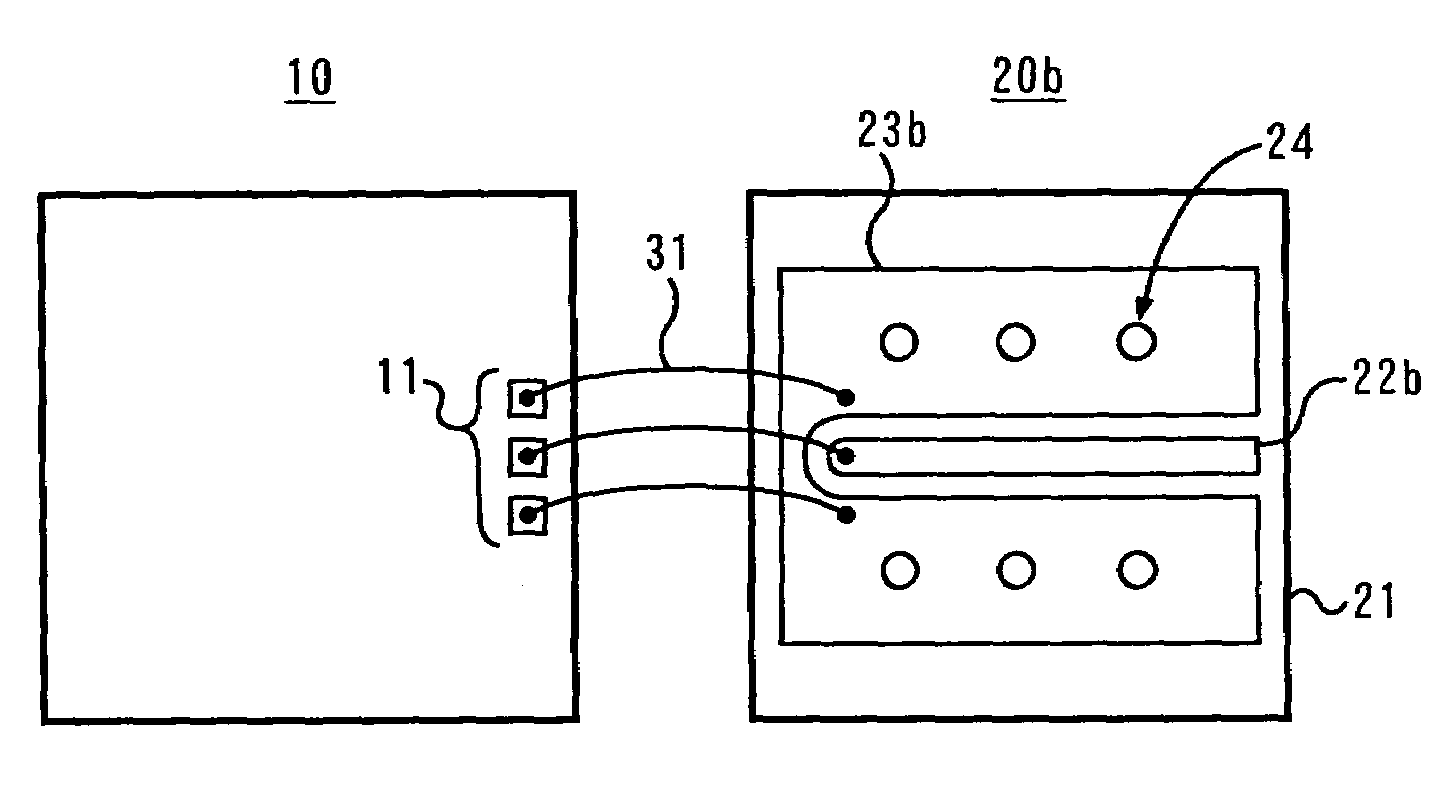
[0045]FIG. 4A is a plan view of a device with a transmission line 20c according to the third embodiment of the present invention. The transmission line 20c has a signal line 22c having an end to which the metal wire 31 is bonded. A ground pattern 23c formed on the signal line substrate 21 has two parallel portions and an intermediate portion connecting the parallel portions. The intermediate portion is interposed between the component 10 and the signal line 22c, and is located below the metal wire 31 that connects the signal line 22c to the pad 11 of the component 10.
[0046]This arrangement of the intermediate portion is similar to the portion B of the ground pattern 23a. The two parallel portions of the ground pattern 23c are not associated with the signal line 22c in signal transmission but are used to ground the intermediate portion that crosses the wires. The two par...
fourth embodiment
[0049]According to a fourth embodiment of the invention, a ground pattern used to make additional capacitance C2 is provided on a side surface of the transmission line substrate 21.
[0050]FIG. 5A is a plan view of a device having a transmission line 20d according to the fourth embodiment of the present invention, and FIG. 5B is a cross-sectional view taken along a line A–A′ shown in FIG. 5A. The transmission line 20d has the signal line 22 and a ground pattern 23 having two parallel portions on either side of the signal line 22. The two parallel portions are associated with the signal line 22 in signal transmission. The through holes 24 electrically connect the ground patterns 23 to the frame 30. A round pattern 26 for making an additional capacitance 2 that should be connected in parallel with the capacitance C1 is provided on a side surface of the signal transmission substrate 21 that faces the component 10. The ground pattern 26 is interposed between the component 10 and the trans...
PUM
 Abstract
Description
Claims
Application Information