Optical module and communication equipment

A technology of optical modules and signal keys, applied in the field of optical communication, can solve problems such as reduced sensitivity, signal integrity problems, poor eye diagrams, etc., and achieve the effect of reducing impedance discontinuities and improving integrity

Pending Publication Date: 2020-03-13
LITUREX GUANGZHOU CO LTD
View PDF0 Cites 3 Cited by
  • Summary
  • Abstract
  • Description
  • Claims
  • Application Information

AI Technical Summary

Problems solved by technology

see figure 1 and figure 2 , which are respectively the traditional BOX package structure and the COB structure. It can be seen that in the BOX package structure, due to the step structure 101 inside the BOX, the height of the electric chip 102 and the gold wire bonding pad 103 can be basically flush, so that the gold wire The length of the line 104 can be extremely short; and in the COB structure (taking the substrate as the circuit board 200 as an example), the bonding pad 203 is on the surface of the circuit board 200, and the chip 202 is also attached to the circuit board 200, so that the chip 202 There is a difference in height between the bonding pad 205 and the bonding pad 203 on the circuit board 200. Due to the process characteristics of the gold wire 204, this height difference will inevitably cause the length of the gold wire 204 to increase, which in turn will affect the quality of the high-speed line. Impedance continuity, causing signal integrity issues
In terms of the overall performance of the optical module, it shows poor eye pattern and reduced sensitivity.
exist figure 2 On the high-speed signal line path of the optical module with a typical COB structure shown, both sides of the bonding gold wire 204 and both sides of the capacitor 206 are locations where impedance discontinuities are generated, which will jeopardize signal integrity.

Method used


Image

  • Optical module and communication equipment
  • Optical module and communication equipment
  • Optical module and communication equipment

Examples


Embodiment Construction

[0021] In order to describe the technical content and structural features of the present invention in detail, further description will be given below in conjunction with the implementation and accompanying drawings.

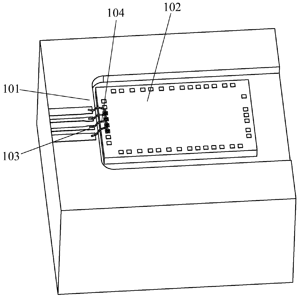
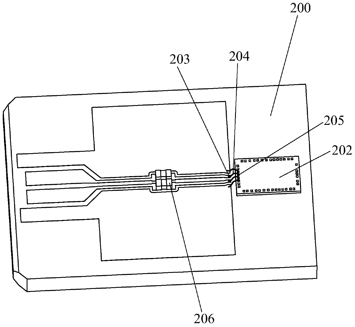
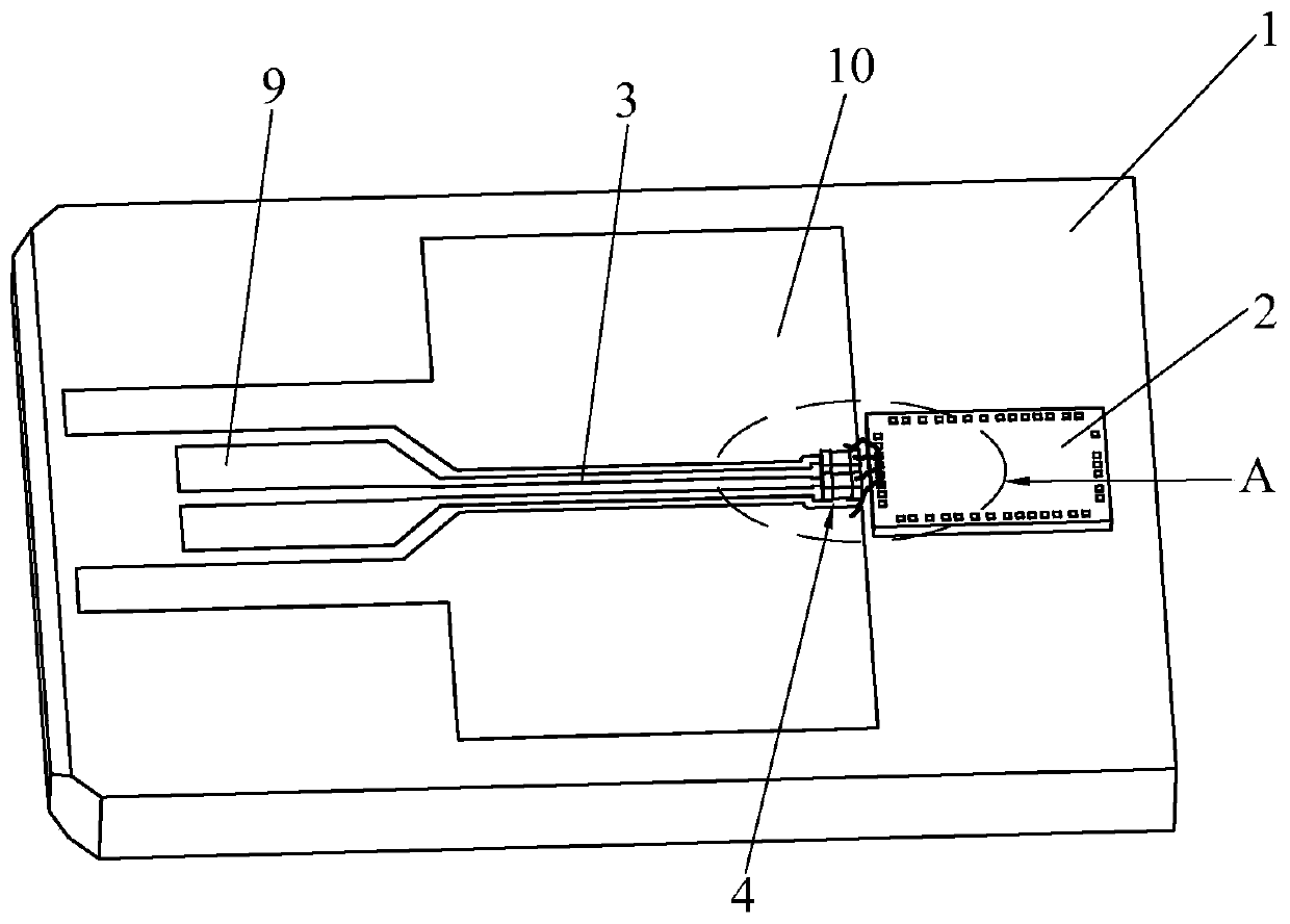
[0022] see Figure 3 to Figure 6 , the invention discloses an optical module, comprising a substrate 1, an electric chip 2, a high-speed signal line 3 and a capacitor 4 / 5, the electric chip 2, a high-speed signal line 3 and a capacitor 4 / 5 are arranged on the substrate 1, and the capacitor 4 / 5 5 is connected between the electric chip 2 and the high-speed signal line 3, the capacitor 4 / 5 includes the first pole plate 41 / 51 and the second pole plate 42 / 52, the first pole plate 41 / 51 is connected to the electric The corresponding pad 21 of the chip 2 is connected, and the second plate 42 / 52 is connected to the high-speed signal line 3 . Generally speaking, the signal bonding wire 6 is bonded on the upper surface of the first plate 41 / 51 , but not limited theret...


PUM


Abstract

The invention discloses an optical module and communication equipment. The optical module comprises a substrate, an electric chip, a high-speed signal line and a capacitor. The electric chip, the high-speed signal line and the capacitor are arranged on the substrate. The capacitor is connected between the electric chip and the high-speed signal line. The capacitor comprises a first pole plate anda second pole plate. The first pole plate is connected with a corresponding bonding pad of the electric chip through a signal bonding line, and the second pole plate is connected with the high-speed signal line. The mode in which the electric chip is directly connected to the capacitor through the bonding line and the capacitor is then connected to the high-speed signal line instead of the mode inwhich the electric chip is connected to the high-speed signal line through the bonding line and the capacitor is arranged in the middle section of the path of the high-speed signal line is adopted. Therefore, the number of impedance discontinuity points on a high-speed signal transmission path is reduced, and the integrity of a high-speed signal is improved.

Description

technical field [0001] The invention relates to the technical field of optical communication, in particular to an optical module and communication equipment. Background technique [0002] With the rapid development of modern optical fiber communication, the optical transmission rate is increasing rapidly, especially under the demand of 5G system, the signal rate of optical devices is getting higher and higher, and the power consumption of optical devices is required to be lower and the price is lower. So the optical module of COB (CHIP ONBOARD) structure began to be popular. The characteristic of COB optical module structure is that it is simple, and all optical and electrical devices are placed on the substrate (the substrate can be a circuit board or a metal plate). In this way, the box body and process for packaging the OSA are omitted, which greatly simplifies the structure. However, the overly simple structure brings new problems. No matter what the structure is, there...

Claims


Application Information

Patent Timeline
Patent Type & Authority Applications(China)
IPC IPC(8): G02B6/42H04B10/27
CPCG02B6/4274H04B10/27
Inventor 黄愚周斌陈骁李海坚黄旭
Owner LITUREX GUANGZHOU CO LTD
Why Eureka
Try Eureka