Test structure embedded in a shipping and handling cover for integrated circuit sockets and method for testing integrated circuit sockets and circuit assemblies utilizing same

a technology of integrated circuit sockets and testing structures, which is applied in the direction of electrical connection testing, measurement devices, instruments, etc., can solve the problems of “open” defects, interfere with the success of capacitive lead-frame testing, and lack of capacitive coupling between an ic lead-frame and a tester's sense pla

Inactive Publication Date: 2006-06-27
AGILENT TECH INC
View PDF11 Cites 45 Cited by
  • Summary
  • Abstract
  • Description
  • Claims
  • Application Information

AI Technical Summary

Problems solved by technology

Note, however, that one of the leads 108 is not soldered to the printed circuit board, thereby resulting in an “open” defect.
If Csense is chosen to be significantly larger than any possible CJoint, a bad lead will result in the AC detector seeing a capacitance near CJoint.
Over the years, various factors have interfered with the success of capacitive lead-frame testing.
One factor is a lack of capacitive coupling between an IC lead-frame and a tester's sense plate.
This problem is largely traced to the on-going miniaturization of IC packages and their lead-frames, as well as the imposition of ground shield and heat sinks between lead-frames and the sensor plate (some of which are internal to an IC's package).
However, they can also interfere with capacitive lead-frame testing in that they sometimes make it difficult to position the sense plate of a capacitive lead-frame tester in close enough proximity to their lead-frames.
Another factor that has interfered with the success of capacitive lead-frame testing is the ratio of non-signal leads to total leads on an IC package.
Capacitive lead-frame testing is not designed to detect opens on such leads.
Thus, a significant fraction of IC leads could suffer from opens that cannot be tested.
Yet another factor that has interfered with the success of capacitive lead-frame testing is socket-mounted IC packages.
This adds a layer of complexity to testing in that proper connection between the board and package requires proper connection between the board and socket.
However, all of these techniques depend on the inserted device's inherent testability for opens coverage; and even if the inserted device is suited to application of these techniques, only signal leads will be adequately tested, and redundant power and ground connections will only be “grossly” tested.
If the inserted device has poor testability, neither the inserted device nor the socket will be adequately tested.
Also, sockets are easily damaged, so there are opportunities to damage a socket that must be minimized during manufacture, shipping, handling, attachment to the printed circuit board, testing or during insertion of the IC into the socket.

Method used


Image

  • Test structure embedded in a shipping and handling cover for integrated circuit sockets and method for testing integrated circuit sockets and circuit assemblies utilizing same
  • Test structure embedded in a shipping and handling cover for integrated circuit sockets and method for testing integrated circuit sockets and circuit assemblies utilizing same
  • Test structure embedded in a shipping and handling cover for integrated circuit sockets and method for testing integrated circuit sockets and circuit assemblies utilizing same

Examples


Embodiment Construction

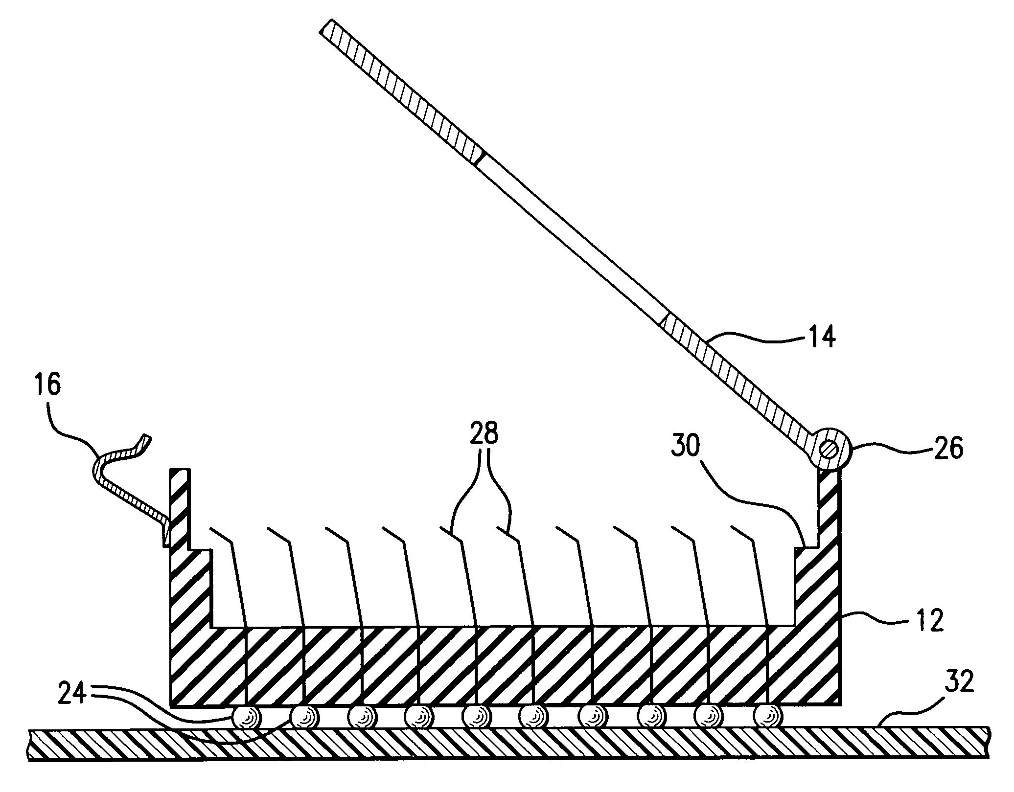
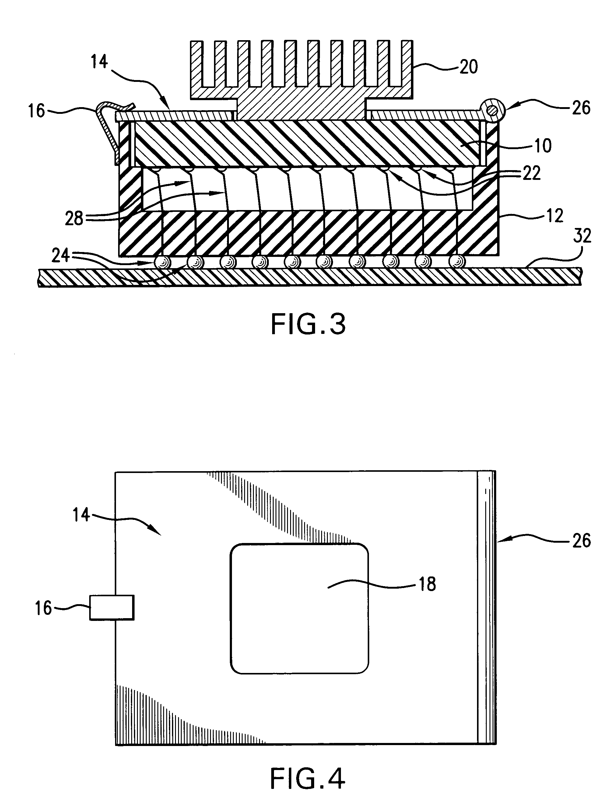
[0028]Some complex integrated circuits are not directly mounted on boards, but are intended to reside in sockets that permit them to be added or replaced after a board is manufactured. An exemplary IC mounted to a board via a socket connector is illustrated in FIGS. 3 and 4, in which an IC 10 is secured in a socket base 12 by means on a lid or clamp plate 14 and a clamp or lock 16. The IC 10 is clamped or locked into place within the socket 12 by a clamp plate 14, which depresses the IC 10 onto a field of contact pin spring fingers 28 that map one-to-one to solder balls (or pins) 24 on the bottom of the socket 12, as shown in FIG. 3. The IC 10 may make electrical contact with a board (not shown) via hundreds or thousands of delicate pin spring fingers 28. The IC 10 may have an array of pads, pins, solder balls or solder columns 22 that come into physical and electrical contact with individual pin spring fingers 28, which map to an array of pads, pins, solder balls or solder columns ...


PUM


Abstract

A device for enabling testing of electrical paths through a circuit assembly is presented. The device may include a test facilitating shipping and handling cover for a socket of the circuit assembly. The test facilitating shipping and handling cover may have a conductive layer for capacitively coupling to an array of pins in the socket during testing. A method for testing continuity of electrical paths through a circuit assembly is presented. In the method, one or more nodes of the circuit assembly are stimulated, contacts of a socket on the circuit assembly are capacitively coupled with a conductive layer of a shipping and handling cover mated with the socket, and an electrical characteristic is measured by a tester coupled to the shipping and handling cover to determine continuity of electrical paths through the circuit assembly.

Description

BACKGROUND OF THE INVENTION[0001]During manufacture, circuit assemblies (e.g., printed circuit boards and Multi-Chip Modules) need to be tested for interconnect defects such as open solder joints, broken connectors, and bent or misaligned leads (e.g., pins, balls, or spring contacts). One way to test for such defects is via capacitive lead-frame testing. FIGS. 1 & 2 illustrate an exemplary setup for capacitive lead-frame testing. FIG. 1 illustrates a circuit assembly 100 comprising an integrated circuit (IC) package 102 and a printed circuit board 104. Enclosed within the IC package is an IC 106. The IC is bonded to the leads 108, 110 of a lead-frame via a plurality of bond wires 112, 114. The leads, in turn, are meant to be soldered to conductive traces on the printed circuit board. Note, however, that one of the leads 108 is not soldered to the printed circuit board, thereby resulting in an “open” defect.[0002]Positioned above the IC package 102 is a capacitive lead-frame test ass...

Claims


Application Information

Patent Timeline
Patent Type & Authority Patents(United States)
IPC IPC(8): G01R31/28G01R31/02G01R31/04G01R31/312
CPCG01R31/312G01R31/046G01R31/70
Inventor PARKER, KENNETH P.
Owner AGILENT TECH INC
Why Eureka
Try Eureka