Electro-optical device substrate, electro-optical device, and electronic apparatus

a technology of electrooptical devices and substrates, applied in the direction of static indicating devices, identification means, instruments, etc., can solve the problems of large wiring resistance, irregular display, scattering display images, etc., and achieve no crosstalk, small wiring resistance of wiring, and good display

Active Publication Date: 2006-06-27
SHENZHEN CHINA STAR OPTOELECTRONICS TECH CO LTD
View PDF13 Cites 9 Cited by
  • Summary
  • Abstract
  • Description
  • Claims
  • Application Information

AI Technical Summary

Benefits of technology

[0027]In the above-stated electro-optical device having a counter substrate, it is preferable that the electro-optical material be liquid crystal. The electro-optical device is a so called liquid crystal device. Applying the present invention to this liquid crystal device maintains small wiring resistance of the wiring to an electrode for applying an electric field to the liquid crystal layer, thereby obtaining good display with no crosstalk.
[0028]An electronic apparatus according to the present invention is characterized by having the above-configured electro-optical device, and a control means for controlling the operation of the electro-optical device. Although the electro-optical device included in this electronic apparatus has a narrow frame region, clear display can be obtained with no crosstalk. It allows a small space where the electro-optical device should be disposed, and also allows information on the electronic apparatus to be displayed clearly.
[0029]In addition, in the electro-optical device substrate according to the present invention, it is preferable that the longer a length in the plurality of wirings from the first side to the second side, the larger a wiring width of the entire region. By doing so, wiring resistance of respective wirings is reduced and also resistance between respective wirings becomes uniform.
[0030]Therefore, when the electro-optical device is manufactured using the electro-optical device substrate, an irregularity in display on the electro-optical device can be reduced.
[0031]In addition, in the electro-optical device according to the present invention, a counter substrate can be prepared opposing the electro-optical device substrat...

Problems solved by technology

However, since reducing the wiring width and the wiring gap depending on a narrow wiring space and an increased wiring number as described above increases the wiring resistance, crosstalk is generated, thereby scattering the display image.
Since the...

Method used


Image

  • Electro-optical device substrate, electro-optical device, and electronic apparatus
  • Electro-optical device substrate, electro-optical device, and electronic apparatus
  • Electro-optical device substrate, electro-optical device, and electronic apparatus

Examples


first embodiment

an Electro-Optical Device Substrate and An Electro-Optical Device

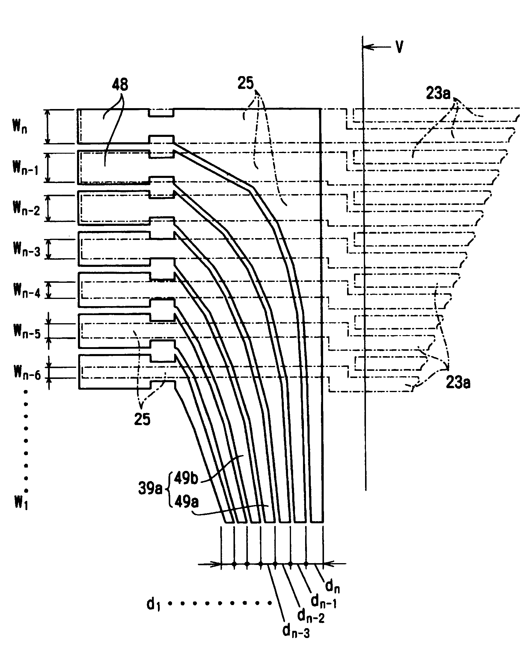
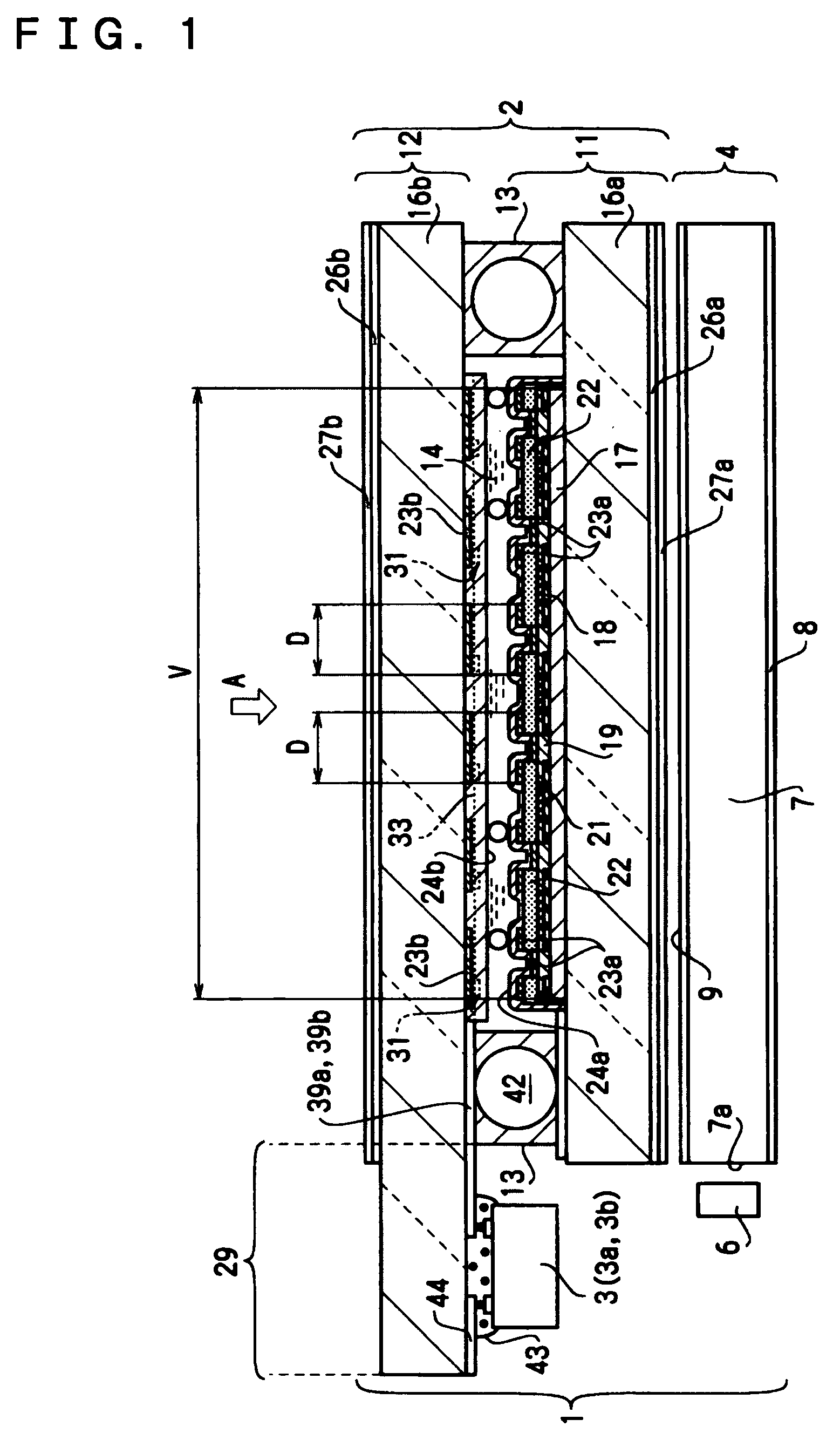
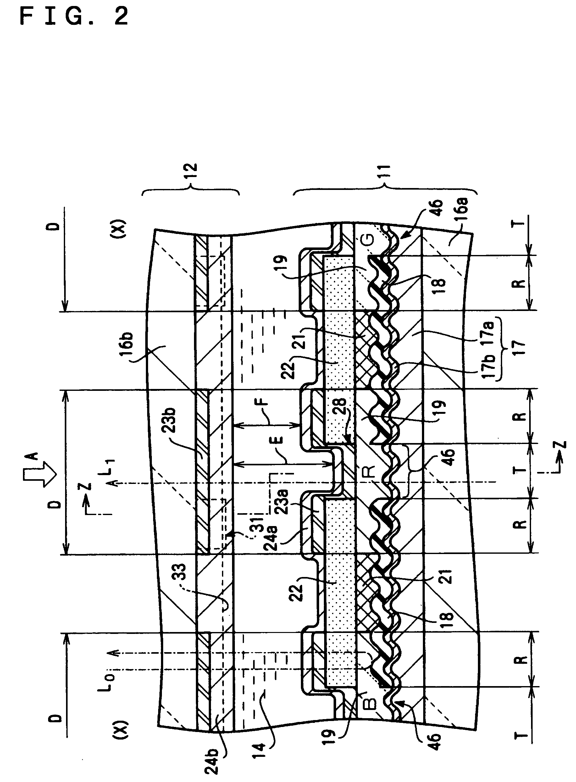
[0052]Hereinafter, a case where the present invention is applied to a liquid crystal device that is an example of the electro-optical device will be described as an example. In addition, the embodiment described below is not intended to limit the present invention as an example of the present invention. In addition, the following explanation is provided with reference to the drawings, if necessary, and in these drawings, in order to indicate important components out of a structure comprising a plurality of components so that it is easily understood, each component is indicated with relative dimensions rather than real dimensions.

[0053]FIG. 1 illustrates an embodiment in which an electro-optical device according to the present invention is applied to a liquid crystal device that is an example thereof. In addition, the liquid crystal device mentioned herein, which is an active matrix type using TFD (Thin Film Diode) bein...


PUM


Abstract

An electro-optical device substrate is provided comprising a base, and a plurality of wirings formed on the base. In at least one of the wirings, there is, in a bent portion of the wirings, a portion whose line width W0 gradually increases from a first side of the base to a second side. By preparing a portion having a large line width lowers the wiring resistance of the wirings, thereby preventing crosstalk from being generated in a display region of the electro-optical device.

Description

RELATED APPLICATIONS[0001]The present application claims priority to Japanese Patent Application Nos. 2003-014733 filed Jan. 23, 2003 and 2003-377171 filed Nov. 6, 2003 which are expressly incorporated by reference in their entireties.BACKGROUND OF THE INVENTION[0002]1. Technical Field[0003]The present invention relates to an electro-optical device substrate used in an electro-optical device, such as a liquid crystal device, an EL device or the like, an electro-optical device using the electro-optical device substrate, and an electronic apparatus using the electro-optical device.[0004]2. Related Art[0005]Presently, in various electronic apparatuses such as a cellular phone, a portable information terminal or the like, an electro-optical device such as a liquid crystal device, an EL device or the like is commonly used. For example, the electro-optical device is used as a display for visually displaying many pieces of information on the electronic apparatus. In this electro-optical de...

Claims


Application Information

Patent Timeline
IPC IPC(8): G02F1/136G02F1/1343G02F1/1345G02F1/1362G02F1/1365G09F9/30G09F9/35H01L51/50H05B33/06
CPCG02F1/1345G02F1/13624H01L27/3288H01L27/3276G02F1/1365H10K59/179H10K59/131A01K63/042A01K63/045
Inventor TAGUCHI, SATOSHIMIYAKO, YUICHIROKANEKO, HIDEKI
Owner SHENZHEN CHINA STAR OPTOELECTRONICS TECH CO LTD
Why Eureka
Try Eureka