Low-power bandgap reference circuits having relatively less components

a reference circuit and low-power bandgap technology, applied in the field of bandgap circuits, can solve the problems of bandgap circuits, unpractical drawbacks, and the need for relatively more complex circuit configurations, and achieve the effect of less components and same level of efficiency

Inactive Publication Date: 2006-07-11
ANALOG INTEGRATIONS CORP
View PDF7 Cites 19 Cited by
  • Summary
  • Abstract
  • Description
  • Claims
  • Application Information

AI Technical Summary

Benefits of technology

[0017]It is therefore an object of the present invention to propose two low-power bandgap circuits each having the relatively less components and the same level of efficiency.

Problems solved by technology

When the layouts of the ICs are under considerations, a relatively larger cross measure is needed for such a circuit, and which would become an unpractical drawback of this kind of bandgap circuits.
Besides, the IPTAT and the IPTVBE are generated sequentially in each of this kind of circuits such that a relatively more complex configuration of the circuit is needed when it is compared with one of the first kind of bandgap circuits.
But, the detailed configuration of the bandgap circuits disclosed in the '071 Patent is relatively complex having ten MOSFETs, three BJTs, and two resistors (as shown in FIG. 5 of the '071 Patent).

Method used


Image

  • Low-power bandgap reference circuits having relatively less components
  • Low-power bandgap reference circuits having relatively less components
  • Low-power bandgap reference circuits having relatively less components

Examples


Embodiment Construction

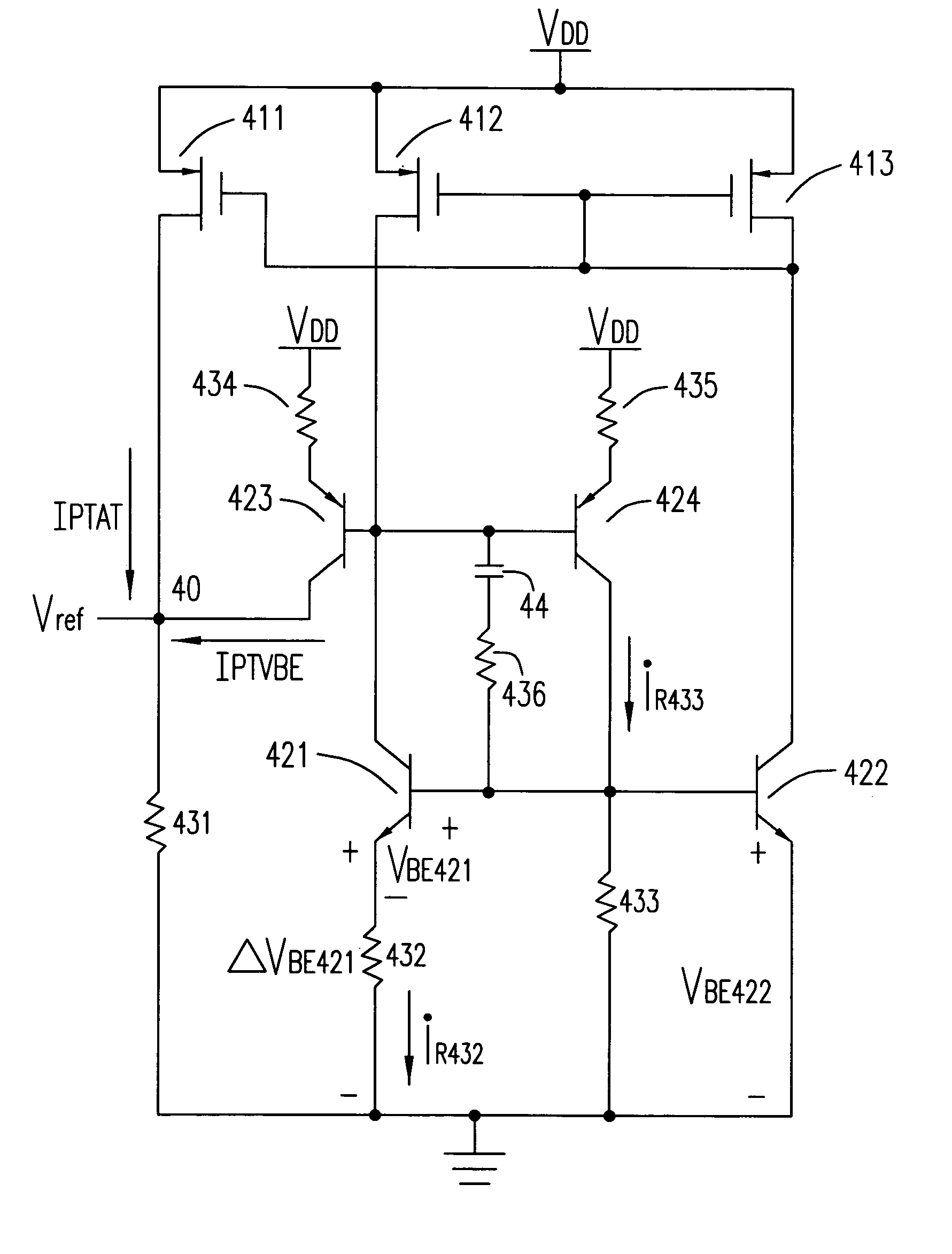
[0040]Please refer to FIG. 4, it shows the schematic circuit diagram of the first preferred embodiment of the proposed low-power bandgap reference circuits of the present invention, which is built up according to the basic configuration of the third kind of lower power bandgap reference circuits (as shown in FIG. 3) each having the relatively less components and the same level of efficiency through employing two different sets of the current mirror circuits. In which, the proportional to absolute temperature (PTAT) current source includes: three same kind of P-type MOSFETs 411–413 (which constitute a first current mirror circuit), two NPN type BJTs 421 and 422, and three resistors 431–433, a square measure of p-n junction of the NPN transistor 421 equals to an integer factor multiplied by a square measure of p-n junction of the NPN transistor 422, and the integer factor is at least 2. Furthermore, the proportional to base-emitter voltage (PTVBE) current source includes: two same kin...


PUM


Abstract

The first proposed circuit includes: a voltage supply; a first current source, including: a first transistor having a first terminal coupled to the voltage supply, a second terminal providing the PTAT current and coupled to an output terminal of the circuit for providing a bandgap reference voltage, and a control terminal; a second current source, including: a first resistor having a first terminal coupled to the voltage supply; and a second transistor having a first terminal coupled to a second terminal of the first resistor, a second terminal providing the PTVBE current and coupled to the output terminal, and a control terminal; and a second resistor having a first terminal coupled to the output terminal, and a second terminal coupled to a common ground. Two current mirror circuits are employed in this circuit.

Description

FIELD OF THE INVENTION[0001]The present invention relates to a bandgap circuit for supplying a reference voltage. More specifically, this invention relates to a bandgap circuit employing the current mirror circuits.BACKGROUND OF THE INVENTION[0002]Please refer to FIG. 1, it shows the schematic circuit diagram of a first kind of low-power bandgap reference voltage circuits of the prior art. In which, the bandgap circuit includes three same kind of P-type MOSFETs 111, 112, 113, an operational-amplifier (op-amp) 12, two PNP type Bipolar Junction Transistors (BJTs) 131 and 132, and four resistors 14, 15, 161, and 162. Furthermore, the resistances of the resistors 161 and 162 are the same, and the cross measure of the p-n junction of the PNP transistor 132 is an integer factor multiplied by the cross measure of the p-n junction of the PNP transistor 131, and the integer factor is at least 2 such that the PNP transistor 132 can be formed by two PNP transistors each having the same cross m...

Claims


Application Information

Patent Timeline
Patent Type & Authority Patents(United States)
IPC IPC(8): G05F3/16G05F3/24G05F3/30H03F3/343
CPCG05F3/30
Inventor FENG, WEI WEN
Owner ANALOG INTEGRATIONS CORP
Why Eureka
Try Eureka