Time limit function utilization

a function and function technology, applied in the field of time limit function utilization apparatus, can solve the problems of large difference in life time, complicated manufacturing method, and difficulty in reproducing accurate holding life tim

Inactive Publication Date: 2006-07-11
KK TOSHIBA
View PDF24 Cites 37 Cited by
  • Summary
  • Abstract
  • Description
  • Claims
  • Application Information

AI Technical Summary

Problems solved by technology

It is therefore difficult to reproduce an accurate holding life time.
In order to form a plurality of memory areas with an arbitrarily set expiration date, memories having gate insulating films with different atomic composition ratios must be formed on a single substrate, which requires a complicated manufacturing method.
Such great variations in leakage current lead to a large difference in the life time, which cannot be permitted in electronic timers.
This is a serious problem in manufacturing an aging device.
When an electronic timer without any battery is implemented using an aging device whose output changes over time, it is difficult to set an accurate operation time because manufacturing variations (of not only the tunnel oxide thickness but also other cell structure parameters) in aging device influence the life time.

Method used


Image

  • Time limit function utilization
  • Time limit function utilization
  • Time limit function utilization

Examples


first embodiment

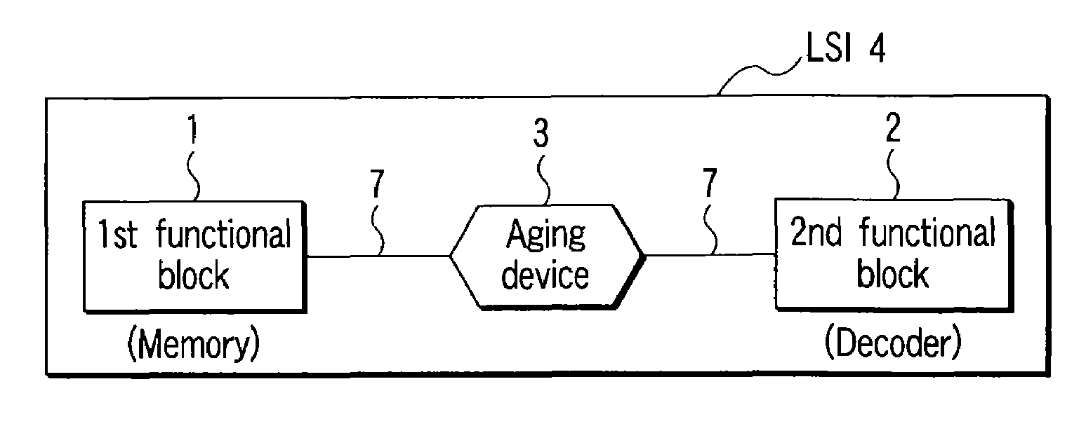
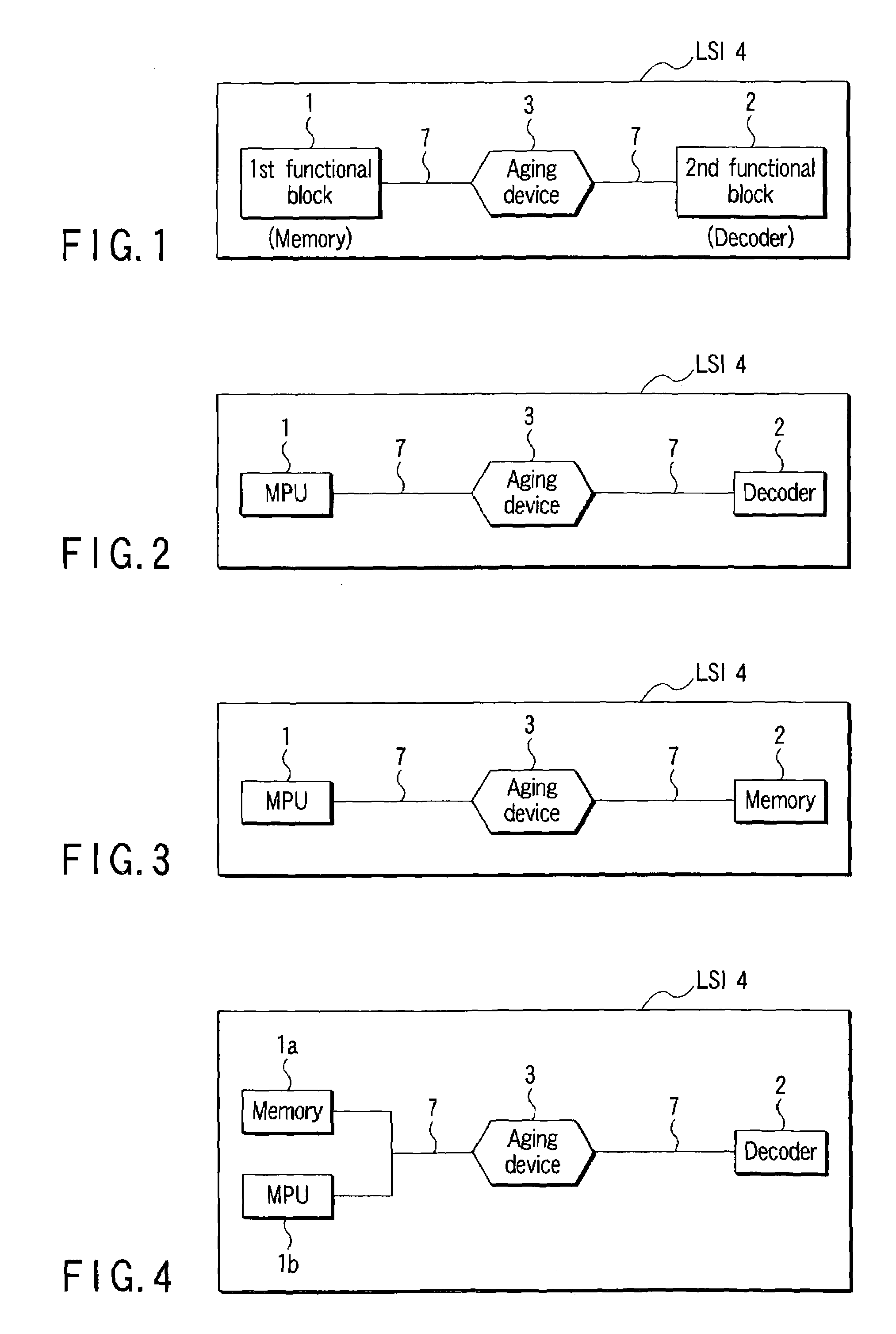
[0170]As shown in FIG. 1, the first embodiment comprises an integrated circuit (LSI) 4 in which a memory area (memory) serving as the first functional block 1, a decoder which serves as the second functional block 2 and reads out information from the memory area, and a semiconductor time switch (automatic turn-off aging device) 3 which is connected between the memory 1 and the decoder 2 via the signal line 7 and turned off upon the lapse of a predetermined time are integrated.

[0171]As shown in FIG. 1, the aging device 3 is interposed between the memory 1 and the decoder 2. In this case, one terminal of the aging device 3 is connected to the memory 1, and the other terminal is connected to the decoder 2. The decoder 2 and memory 1 can access each other.

[0172]The aging device 3 is turned off upon the lapse of a predetermined time, and the memory 1 and decoder 2 are disconnected from each other. The decoder 2 cannot access the memory 1, and the LSI 4 malfunctions. For example, when the...

second embodiment

[0173]As shown in FIG. 2, the second embodiment comprises an integrated circuit (LSI) 4 in which an operational area (MPU) 1 serving as the first functional block, a decoder 2 serving as the second functional block, and a semiconductor time switch (aging device) 3 which is connected between the MPU 1 and the decoder 2 via the signal line 7 and turned off upon the lapse of a predetermined time are integrated.

[0174]As shown in FIG. 2, the aging device 3 is interposed between the MPU 1 and the decoder 2. In this case, one terminal of the aging device 3 is connected to the MPU 1, and the other terminal is connected to the decoder 2. The MPU 1 and decoder 2 can access each other.

[0175]The aging device 3 is turned off upon the lapse of a predetermined time, and the MPU 1 and decoder 2 are disconnected from each other. The MPU 1 and decoder 2 cannot access each other, and the LSI 4 malfunctions. For example, encryption information decrypted by the MPU 1 cannot be read by the decoder 2, and...

third embodiment

[0176]As shown in FIG. 3, the third embodiment comprises an integrated circuit (LSI) 4 in which an operational area (MPU) 1 serving as the first functional block, a memory area (memory) 2 serving as the second functional block, and a semiconductor time switch (aging device) 3 which is connected between the MPU 1 and the memory 2 via the signal line 7 and turned off upon the lapse of a predetermined time are integrated.

[0177]As shown in FIG. 3, the aging device 3 is interposed between the MPU 1 and the memory 2. In this case, one terminal of the aging device 3 is connected to the MPU 1, and the other terminal is connected to the memory 2. The MPU 1 and memory 2 can access each other.

[0178]The aging device 3 is turned off upon the lapse of a predetermined time, and the MPU 1 and memory 2 are disconnected from each other. The MPU 1 and memory 2 cannot access each other, and the LSI 4 malfunctions. For example, the MPU 1 cannot read a decryption key stored in the memory 2, and a time li...


PUM


Abstract

A time limit function utilization apparatus includes a first function block, a second function block, a signal line which connects the first and second function blocks and allows using a desired function that is generated by accessing the first and second function blocks with each other, and a semiconductor time switch interposed in or connected to the signal line, and disables or enables mutual access between the first and second function blocks upon the lapse of a predetermined time.

Description

CROSS-REFERENCE TO RELATED APPLICATIONS[0001]This application is based upon and claims the benefit of priority from the prior Japanese Patent Applications No. 2002-198144, filed Jul. 8, 2002; No. 2002-336961, filed Nov. 20, 2002; and No. 2003-188792, filed Jun. 30, 2003, the entire contents of all of which are incorporated herein by reference.BACKGROUND OF THE INVENTION[0002]1. Field of the Invention[0003]The present invention relates to a time limit function utilization apparatus, particularly, to a semiconductor integrated circuit formed from an age-based change device (aging device) whose output changes over time and a circuit technology controlling the life time of the aging device, more particularly, to an integrable electronic timer which accurately operates in an off-line state in which the timer is disconnected from a battery.[0004]2. Description of the Related Art[0005]A security system which sets an expiration date on a cipher or password has widely been used. For example,...

Claims


Application Information

Patent Timeline
Patent Type & Authority Patents(United States)
IPC IPC(8): G01R19/00H01L27/115G04F10/10G06F1/00G06F9/38G06K19/07G06K19/073G07C9/00G07F7/10G11C16/14H01L21/77H01L27/105H03K17/00H03K17/284
CPCG01R31/2642H01L29/7883G06K19/0723G06K19/073G06K19/07372G06Q20/341G07C9/00111G07F7/082G07F7/084G07F7/1008H01L21/28273H01L27/115H01L29/42324H01L29/66825G06F9/3802G06F2221/2137G07C2009/00976G11C16/14G11C16/349H01L27/11558H01L29/40114G07C9/28H10B41/60H10B69/00
Inventor WATANABE, HIROSHIMATSUZAWA, KAZUYASHIROTA, RIICHIRO
Owner KK TOSHIBA
Why Eureka
Try Eureka