Self-aligned split-gate nonvolatile memory structure and a method of making the same

a nonvolatile memory and split-gate technology, applied in semiconductor devices, electrical apparatus, transistors, etc., can solve the problems of alignment of various functional elements, large size of a corresponding, and lower endurance, so as to improve program/erase efficiency, endurance characteristics and device-to-device uniformity, and the effect of increasing the control of tunneling and interpoly oxides

Inactive Publication Date: 2006-07-18
SAMSUNG ELECTRONICS CO LTD
View PDF14 Cites 20 Cited by
  • Summary
  • Abstract
  • Description
  • Claims
  • Application Information

AI Technical Summary

Benefits of technology

[0024]Exemplary embodiments of split-gate transistors according to the present invention provide self-alignment of the control gates and floating gates and provide an increased degree of control over the tunneling and interpoly oxides. These process and structural improvements translate into improved program / erase efficiency, endurance characteristics and device-to-device uniformity.

Problems solved by technology

Split-gate memory cell transistors also have several disadvantages including a larger size than a corresponding flash cell and lower endurance than a corresponding EEPROM (electrically erasable programmable read only memory) utilizing F-N (Fowler-Nordheim) tunneling injection.
A problem associated with the manufacture of floating gate memory cell arrays has been the alignment of the various functional elements including the source, drain(s), control gate(s), and floating gate(s).
The proper relative alignment and orientation of the various memory cell elements results in increased manufacturing yield, reduced performance distribution and increased reliability of the final semiconductor products.
A problem associated with the manufacture of split-gate memory cells can be a mismatch of the lengths and positioning of the paired control gates.

Method used


Image

  • Self-aligned split-gate nonvolatile memory structure and a method of making the same
  • Self-aligned split-gate nonvolatile memory structure and a method of making the same
  • Self-aligned split-gate nonvolatile memory structure and a method of making the same

Examples


Embodiment Construction

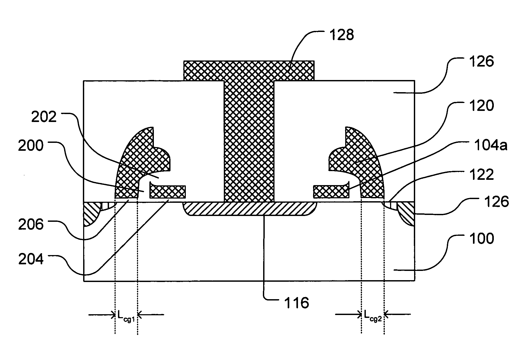
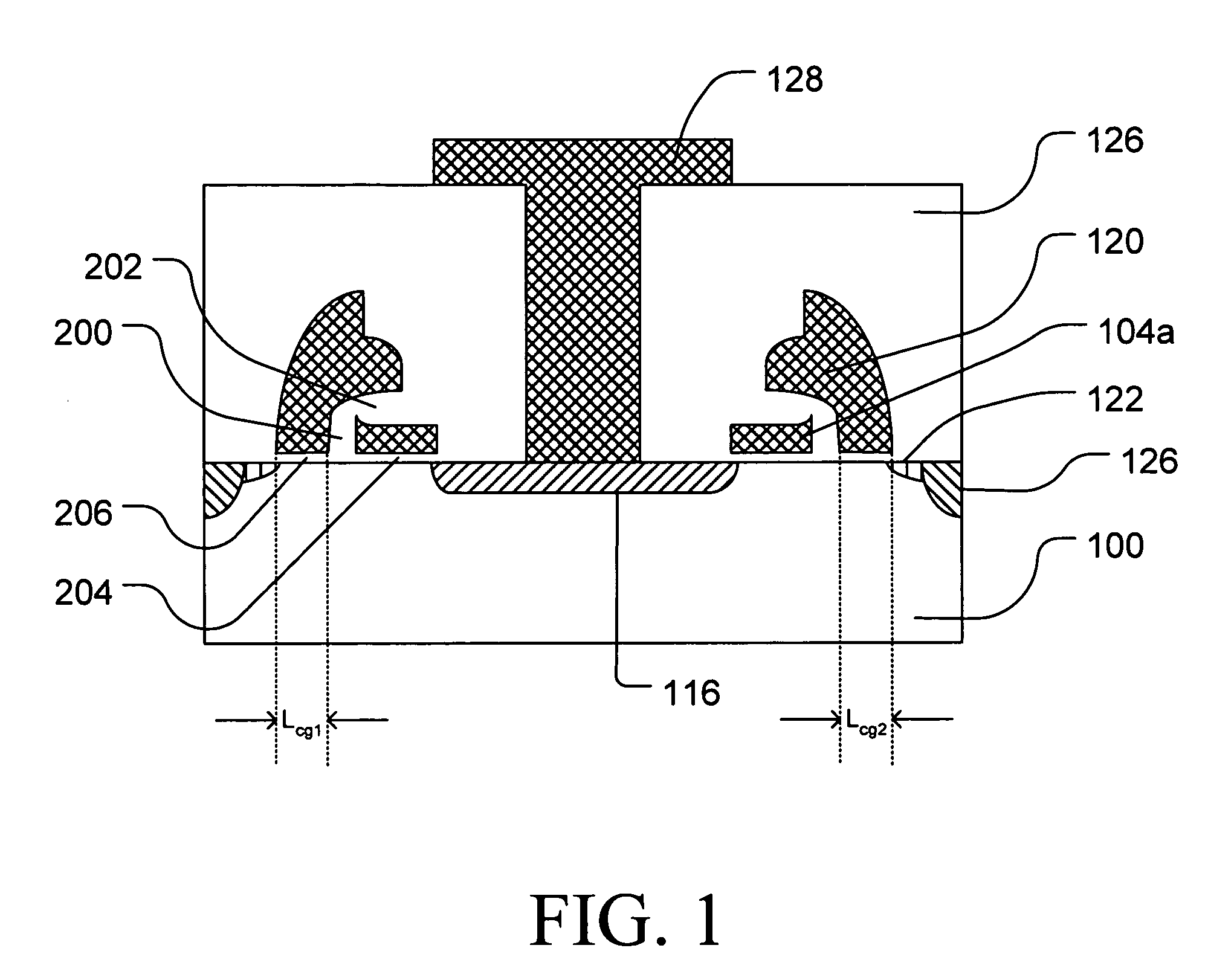
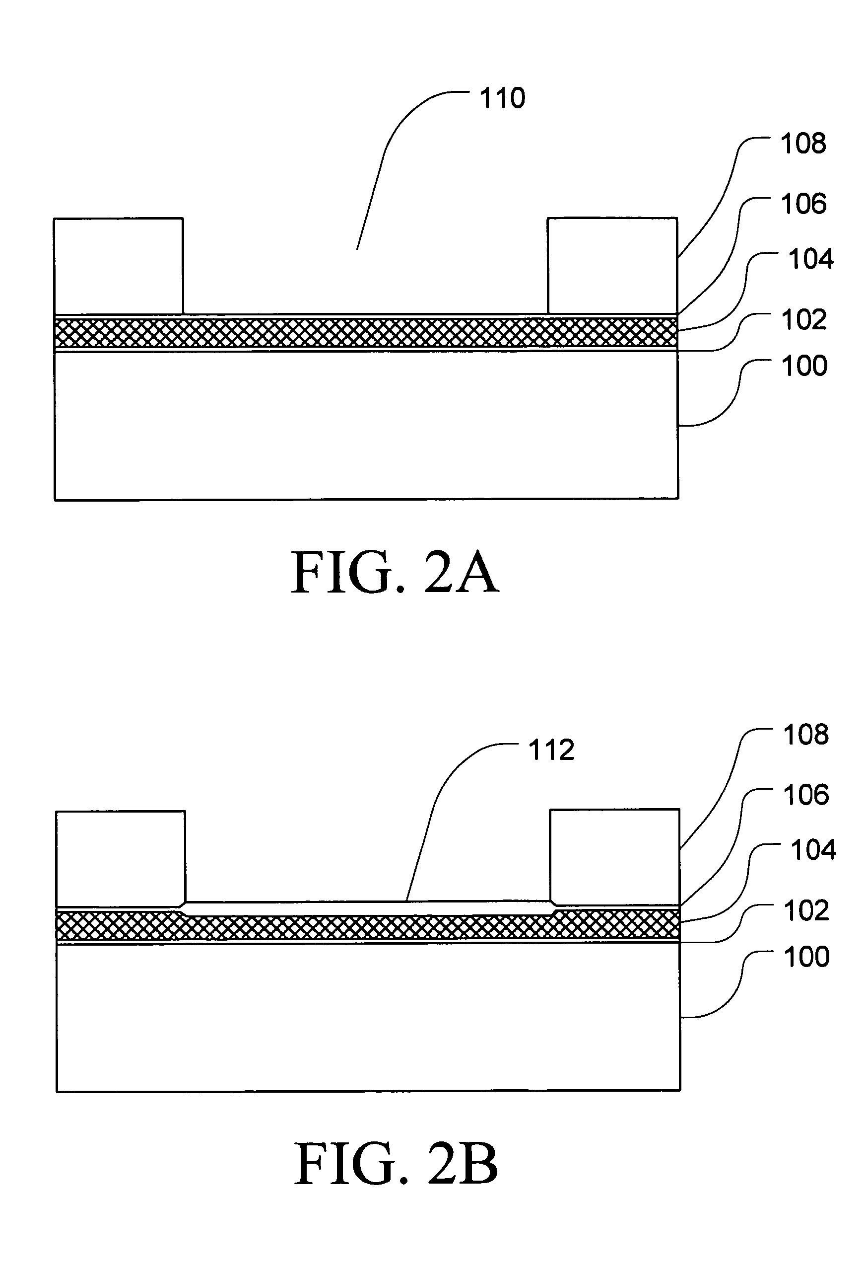
[0032]Exemplary embodiments of a split-gate transistor structure and a method of manufacturing such as split-gate transistor structure according to the present invention will now be described more fully with reference to the accompanying drawings. As will be appreciated, this invention may, however, be embodied in many different forms and should not be construed as being limited to the embodiments set forth herein; rather, these embodiments are provided so that this disclosure will be thorough and complete, and will fully convey the concept of the invention to those of ordinary skilled in the art.

[0033]As used herein, layers or structures described as being “on” or “over” another layer or substrate, need not be formed or deposited directly on the referenced layer or substrate but should be understood to encompass one or more intervening layers. Similarly, when layers or structures are described as being “under” another layer or surface, the layer or structure need not be positioned ...


PUM


Abstract

Provided are non-volatile split-gate memory cells having self-aligned floating gate and the control gate structures and exemplary processes for manufacturing such memory cells that provide improved dimensional control over the relative lengths and separation of the split-gate elements. Each control gate includes a projecting portion that extends over at least a portion of the associated floating gate with the size of the projecting portion being determined by a first sacrificial polysilicon spacer that, when removed, produces a concave region in an intermediate insulating structure. The control gate is then formed as a polysilicon spacer adjacent the intermediate insulating structure, the portion of the spacer extending into the concave region determining the dimension and spacing of the projecting portion and the thickness of the interpoly oxide (IPO) separating the upper portions of the split-gate electrodes thereby providing improved performance and manufacturability.

Description

CROSS REFERENCE TO RELATED APPLICATIONS[0001]This U.S. nonprovisional patent application claims priority under 35 U.S.C. § 119 from Korean Patent Application No. 10-2004-0007230, which was filed on Feb. 4, 2004, in the Korean Intellectual Property Office, the entire contents of which are hereby incorporated by reference.BACKGROUND OF THE INVENTION[0002]1. Field of the Invention[0003]The present invention is directed to split-gate memory cells and semiconductor devices that include such memory cells. More particularly, the present invention is directed to split-gate memory cells in which the floating gate and the control gate are self-aligned with the control gate at least partially overlapping the control gate and a method of manufacturing such split-gate memory cells.[0004]2. Description of the Related Art[0005]Semiconductor memory cells utilizing floating gates that may be charged to alter the performance of the associated channel regions and control gates have been manufactured i...

Claims


Application Information

Patent Timeline
Patent Type & Authority Patents(United States)
IPC IPC(8): H01L21/336H01L21/8247H01L21/8234H01L21/8239H01L27/10H01L27/115H01L29/423H01L29/788H01L29/792
CPCH01L29/42324H01L29/7885H10B69/00H10B41/30
Inventor JEON, HEE SEOGYOON, SEUNG BEOMKIM, YONG TAE
Owner SAMSUNG ELECTRONICS CO LTD
Why Eureka
Try Eureka