Storage device having a resistance measurement system

a technology of resistance measurement and storage device, which is applied in the direction of digital storage, data recording, instruments, etc., can solve the problems of approaching fundamental limits, difficult and expensive task of precisely controlling the spacing between the probe and the storage medium, and becoming increasingly difficult to put more information into storage devices using conventional technologies

Active Publication Date: 2006-08-01
SAMSUNG ELECTRONICS CO LTD
View PDF9 Cites 10 Cited by
  • Summary
  • Abstract
  • Description
  • Claims
  • Application Information

AI Technical Summary

Problems solved by technology

However, it has become increasingly difficult to put more information into storage devices using conventional technologies, which may be approaching fundamental limits.
However, precisely controlling the spacing between the probe and storage medium is a difficult and expensive task.
In each of these configurations, it is difficult and expensive to build a storage system where the storage medium and / or probe are not eventually damaged.
Some approaches are based on non-contact Scanning Force Microscopy (SFM), which typically suffers from poor resolution and poor signal to noise ratio.
Another approach is based on Near-Field Scanning Optical Microscopy, which has limited lateral resolution and slow access times. The utility of the storage device is limited if it takes a long time to retrieve stored information.

Method used


Image

  • Storage device having a resistance measurement system
  • Storage device having a resistance measurement system
  • Storage device having a resistance measurement system

Examples


Embodiment Construction

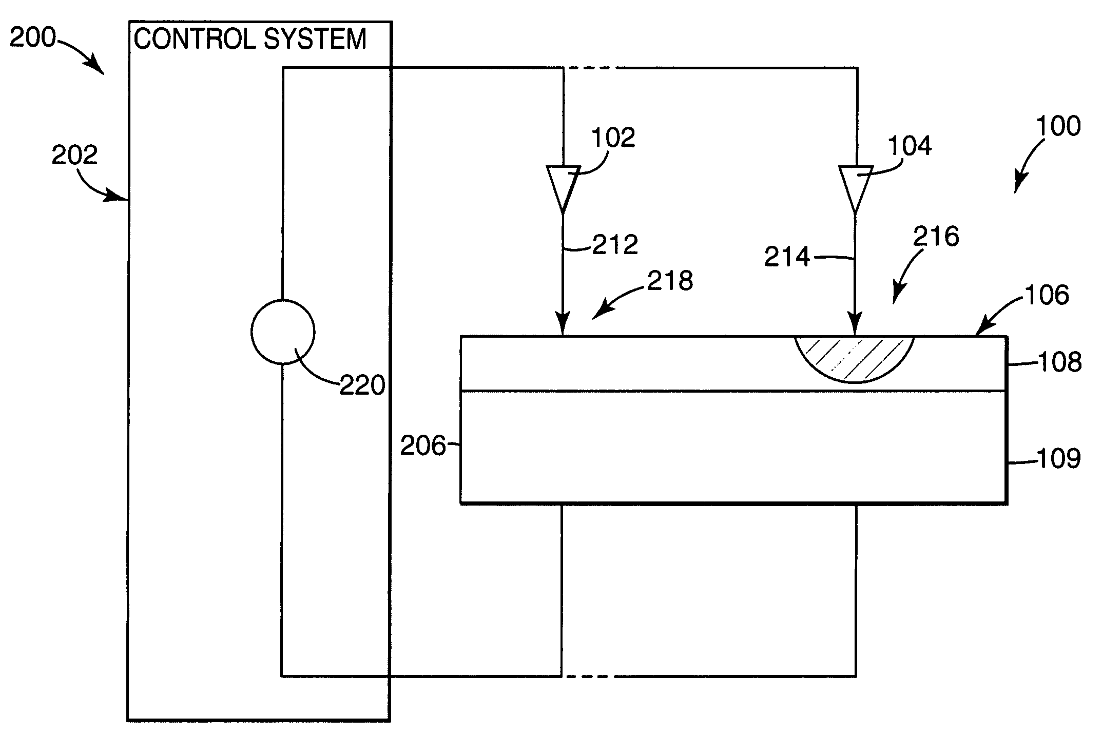
[0017]FIG. 1 is a side cross-sectional view illustrating one exemplary embodiment of a storage device 100, such as an atomic resolution storage device, according to the present invention. The storage device 100 includes a storage medium having an information layer and a semiconductor layer, the information layer having a first state or a second state for storing information at a storage area or location. During a read operation, an electron emitter provides an electron beam to the storage location and an electron beam induced current passes through the storage medium. The device includes a resistance measurement system for detecting the resistance of the storage medium at the storage location using the electron beam-induced current for determining the state of the storage medium at the storage area or location.

[0018]Atomic resolution storage device 100 includes a nonvolatile memory component employing a plurality of electron emitters, one or more storage medium surfaces and at least...


PUM

PropertyMeasurementUnit
resistance measurementaaaaaaaaaa
resistanceaaaaaaaaaa
currentaaaaaaaaaa

Abstract

A storage device and a storage system employing the storage device. In one embodiment, the storage device comprises an electron emitter and a storage medium comprising an information layer having at least a first state and a second state for storing information. The storage device comprises a resistance measurement system coupled to the storage medium for reading the information stored at the information layer by measuring resistance to determine a state of a storage area on the information layer.

Description

BACKGROUND OF THE INVENTION[0001]Researchers have worked for years to increase the storage density and reduce the cost per bit of computer system storage devices. These efforts have met with some success, as storage density has increased and cost per bit has dropped in conventional storage devices, such as magnetic hard-drives, optical drives and dynamic random access memory (DRAM). However, it has become increasingly difficult to put more information into storage devices using conventional technologies, which may be approaching fundamental limits.[0002]Scientists have proposed alternative approaches in an attempt to increase storage density and reduce cost per bit. In one approach, referred to as Scanned Probe Microscopy (SPM), a probe is positioned extremely close to a storage medium. In one configuration, referred to as Scanning Tunneling Microscopy (STM), the probe is positioned within a few nanometers of the storage medium. Positioning the probe close to the storage medium ensu...

Claims


Application Information

Patent Timeline
Patent Type & Authority Patents(United States)
IPC IPC(8): G11C11/00G11B9/00G11B9/04G11B9/10
CPCB82Y10/00G11B9/04G11B9/10G11B9/149G11B9/1409G11B9/1418G11B9/1436G11B9/14
Inventor ASHTON, GARY RAYBICKNELL, ROBERT NEWTON
Owner SAMSUNG ELECTRONICS CO LTD
Why Eureka
Try Eureka