
OLED display with control

a display and control technology, applied in the direction of instruments, static indicating devices, etc., can solve the problems of complex circuit design, undesirable variation in light output from element to element, non-uniformity of oled displays, etc., and achieve the effect of improving performance and simplifying the control structur

Active Publication Date: 2006-08-08
GLOBAL OLED TECH
View PDF15 Cites 181 Cited by
  • Summary
  • Abstract
  • Description
  • Claims
  • Application Information

AI Technical Summary

Benefits of technology

[0024]The present invention provides an OLED control device having

Problems solved by technology

Active-matrix OLED devices suffer from manufacturing variability that leads to non-uniformity in OLED displays.
Moreover, the OLED light-emitting elements themselves degrade over time and with use, thereby modifying the light output from the devices in response to control and power signals.
Hence, conventional active-matrix drive methods that employ stored charge deposited on a local capacitor at each pixel site to control a drive circuit for driving an OLED light-emitting element, will experience an undesirable variation in light output from element to element.
However, such circuit designs are typically complex and employ many more elements and control signals.
Hence, such an approach may reduce manufacturing yields and reduce the light-emissive area of the OLED device.
However, use of current-driven circuits is complex and requires a large amount of space for each pixel in a display device.
The described technique, however, diverts driving current from an OLED, thereby decreasing the operating efficiency of the circuit.
However, when placed in series with an OLED element, transistors will increase the overall voltage necessary to drive the OLED element or may otherwise increase the overall power used by the OLED element or decrease the range of currents available to the OLED element.
An additional problem faced by OLED devices is the change in OLED material characteristics as the OLED elements are used.
Typically, the OLED elements become less efficient and have a higher effective resistance.
Both of these factors tend to increase the voltage needed to drive current through the OLED element.
This increases the overall voltage of the system, inhibiting the brightness of the elements at a given voltage.
Thin-film transistors used to drive a typical active-matrix OLED element also place restrictions on operation.
If control signals move the transistors out of the restricted operating range, the device will no longer behave as desired.

Method used


Image

  • OLED display with control
  • OLED display with control
  • OLED display with control

Examples


Embodiment Construction

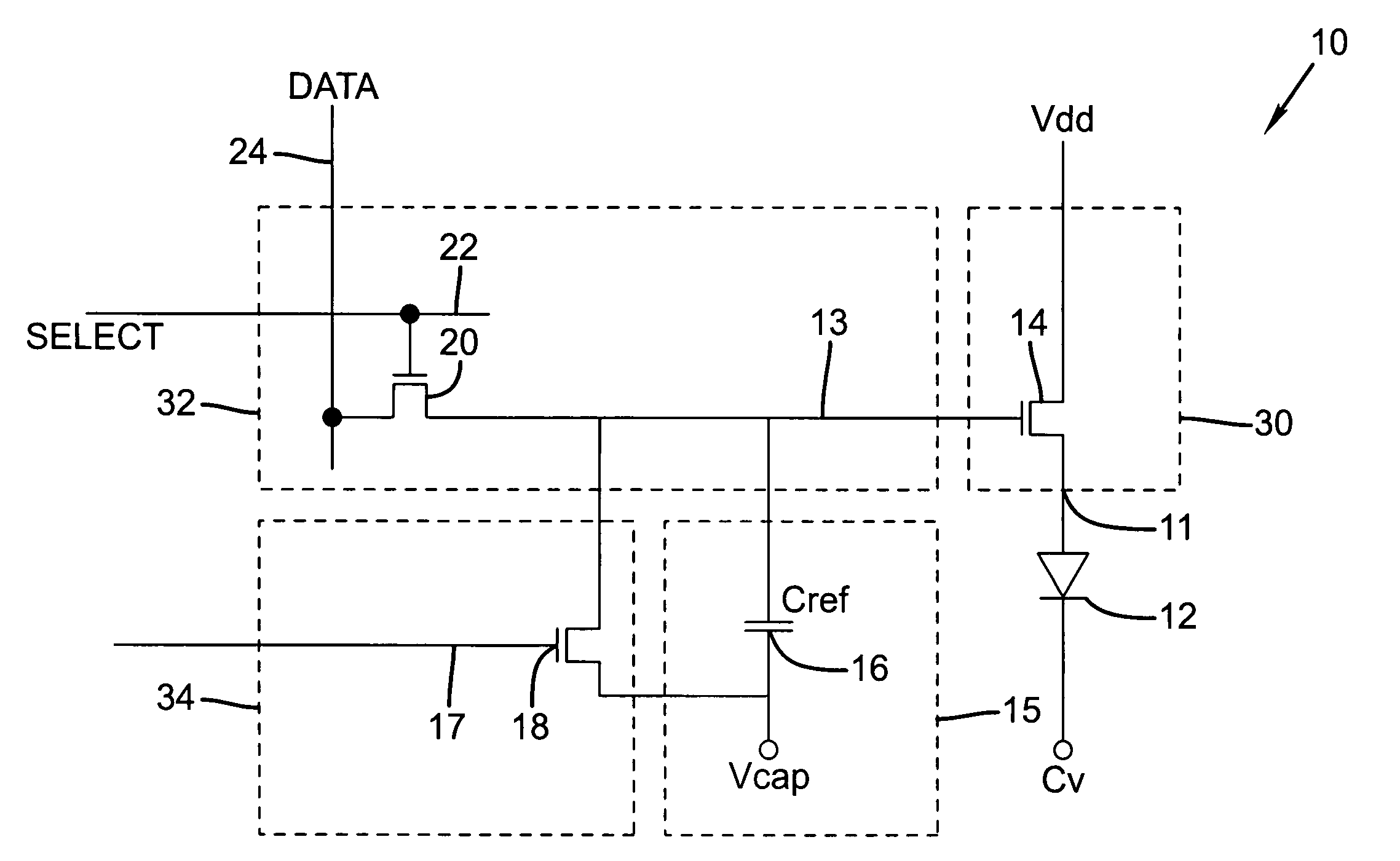
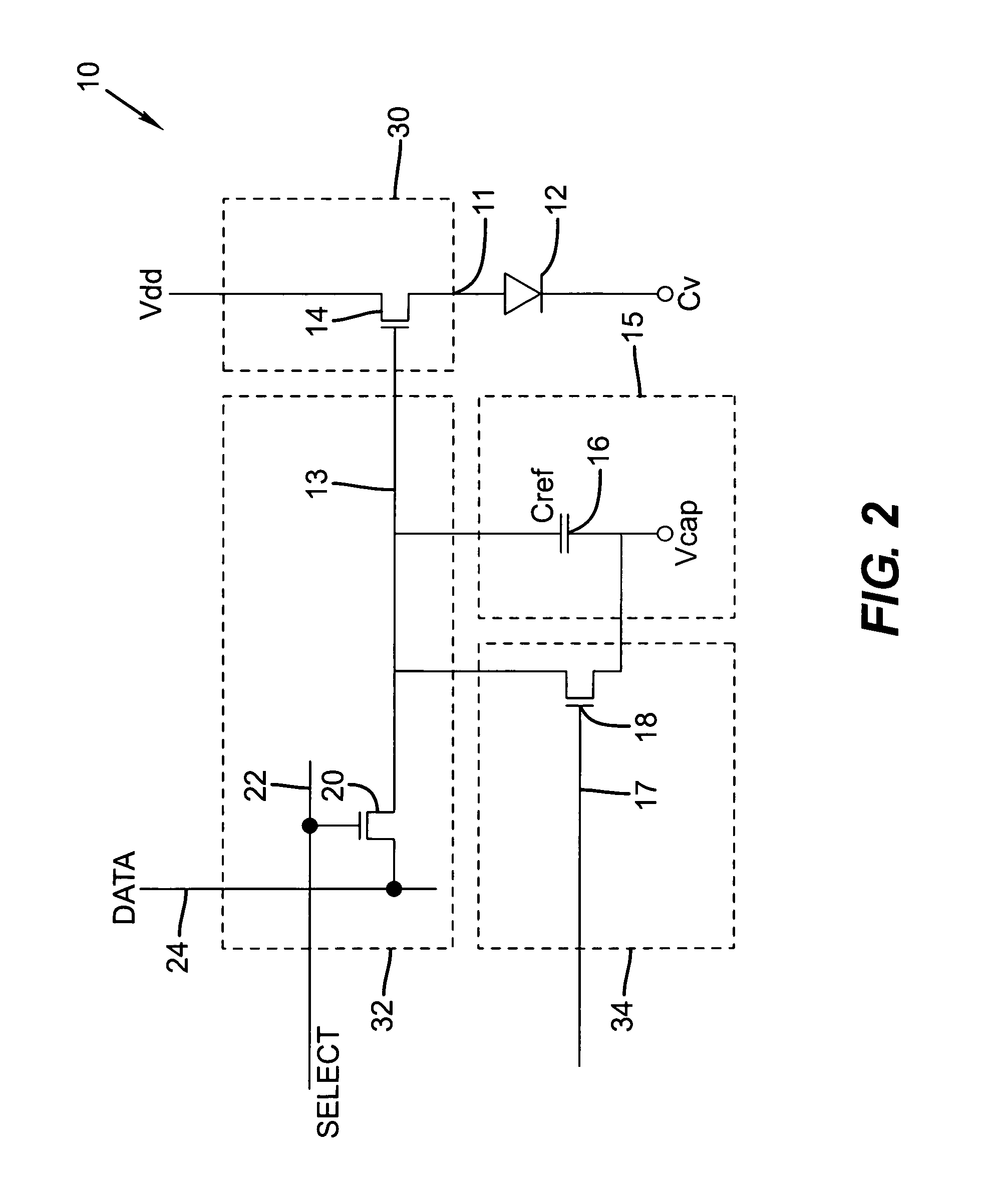
[0025]Referring to FIG. 1, according to one embodiment of the present invention an OLED device and control circuit 10, comprises an OLED 12 responsive to a drive signal 11; a drive circuit 30 connected to the OLED 12 responsive to a charge signal 13 for controlling the drive signal 11; a variable charge storage circuit 15 connected to the drive circuit 30 and providing the charge signal 13; a deposition circuit 32 responsive to deposition signal 22, 24 (e.g., representing select and data control signals) for depositing variable charge in the variable charge storage circuit 15; and a modulation circuit 34 responsive to an external modulation signal 17 for removing charge from the variable charge storage circuit 15. According to the present invention, the charge deposited in the charge storage circuit 15 will vary depending on the desired brightness of the OLED 12. The phase of the external modulation signal 17 with respect to the deposition signals 22 and 24 is also variable. Hence, ...


PUM


Abstract

An OLED device and control circuit, comprising: a) an OLED responsive to a drive signal; b) a drive circuit connected to the OLED responsive to a charge signal for controlling the drive signal; c) one or more variable charge storage capacitors providing the charge signal; d) a deposition circuit for depositing variable charge in the one or more variable charge storage capacitors; and e) a modulation circuit responsive to an external modulation signal for removing charge from the one or more variable charge storage capacitors.

Description

FIELD OF THE INVENTION[0001]The present invention relates to solid-state display devices and means to store and display pixel values and images.BACKGROUND OF THE INVENTION[0002]Solid-state image display devices utilizing light-emissive pixels are well known and widely used. For example, OLED devices are used in flat-panel displays, in both passive- and active-matrix configurations, and in both top-emitter and bottom-emitter designs. Control circuits for OLED displays are also well known in the art and include both voltage- and current-controlled schemes.[0003]Conventional passive-matrix OLED displays employ a variable current in combination with a fixed period during which the OLED light-emitting element emits light. Successive rows or columns of OLED elements are energized and the entire OLED display is refreshed at a rate sufficient to avoid the appearance of flicker. For example, WO2003034389 A2 entitled “System and Method for Providing Pulse Amplitude Modulation for OLED Display...

Claims


Application Information

Patent Timeline
IPC IPC(8): G09G3/10G09G3/30
CPCG09G3/3233G09G3/2011G09G3/2014G09G2300/0842G09G2360/147G09G2310/0251G09G2320/0261G09G2320/0271G09G2320/043G09G2300/0876
Inventor COK, RONALD S.
Owner GLOBAL OLED TECH
Features
  • Generate Ideas
  • Intellectual Property
  • Life Sciences
  • Materials
  • Tech Scout
  • Unparalleled Data Quality
  • Higher Quality Content
  • 60% Fewer Hallucinations
Learn More