Slim USB electronic device

a technology of electronic devices and usb, applied in the direction of electrical discharge lamps, coupling device connections, electric discharge tubes, etc., can solve the problems of reducing the affecting the service life of electronic devices, and affecting the portability of usb electronic devices, so as to achieve more protection

Active Publication Date: 2006-08-15
SONY CORP
View PDF5 Cites 51 Cited by
  • Summary
  • Abstract
  • Description
  • Claims
  • Application Information

AI Technical Summary

Benefits of technology

[0009]A another objective of the invention is to provide an improved USB electronic device, in which the substrate and other electronic elements are substantially enclosed for preventing the connector and the contacts of the USB electronic device to become unnecessarily revealed, thereby gaining more protection.
[0010]A further objective of the invention is to provide an improved USB electronic device, in which every opening corresponds to a metal strip to make the improved USB electronic device functional for guiding each contact of an USB receptacle into the right position, and prevent mutual influences between the two metal strips or short circuit caused by external matter.

Problems solved by technology

Because the USB connector's limitations, however, the USB electronic device will become too thick to be portable.
However, as the connector 202 inserts and pulls out over and over again, the metal film 204 becomes easier to peel off, resulting in the USB storage device being unable to be used.
Besides, most areas of the connector 202 are exposed from the device housing, making the contacts (formed of metal films) short circuit easier by external matter which decrease the electronic device's life.
Although this structure overcomes the problem that the metal film peels off easily, the connector 30 is still exposed to too external matter.
Further, because it's necessary to drill on the connector 30 before adhering the metal strips 33, and a metal housing 39 shaped of U letter is also needed for protecting the connector 30, the structure of the USB electronic device becomes more complicated and harder to fabricate, resulting in difficulties in reducing production costs.

Method used


Image

  • Slim USB electronic device
  • Slim USB electronic device
  • Slim USB electronic device

Examples


Embodiment Construction

[0022]The preferred embodiment of the present invention is now described in great detail. Nevertheless, it should be recognized that the present invention can be practiced in a wide range of embodiments besides those explicitly described, and the scope of the present invention is expressly not limited except as specified in the accompanying claims.

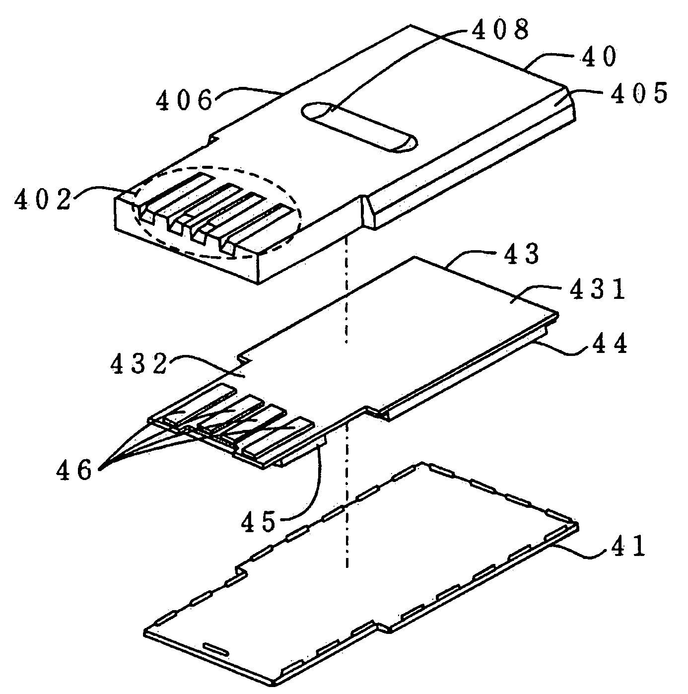
[0023]FIG. 4A illustrates a slim USB electronic device, which is the preferred embodiment of the invention and specially an USB storage device. The arrow indicates the direction of the USB electronic device while inserting into an USB receptacle. The disclosed USB electronic device is enclosed with a housing 4, which opens some openings 402 (four in this embodiment) for exposing inner metal strips 46 as the contact for communicating with the USB receptacle of a host.

[0024]FIG. 4B is the explosion drawing of the preferred embodiment of the invention illustrating in FIG. 4A. Referring to FIG. 4B, the inner structure is distinctly revealed, t...


PUM


Abstract

A slim USB electronic device, which includes a substrate and a housing enclosing the substrate, is disclosed. The substrate includes a circuit board and an extended connector. Electrically conductive metal strips are adhered to the connector, and integrated circuit elements are mounted on the substrate. The housing has openings, through which the corresponding metal strips are exposed and electrically communicate with the contacts of an USB receptacle.

Description

BACKGROUND OF THE INVENTION[0001]1. Field of the Invention[0002]The invention discloses a USB electronic device and specially relates to a slim USB electronic device.[0003]2. Description of the Prior Art[0004]With the progress in the information technology (IT) industry, portable electronic devices become more and more popular. Some of them, such as a flash drive or a small memory card, are capable of communicating with host (PC or notebook computer) through specific transmission interfaces, in which the universal serial bus (USB) is the most popular one. Because the USB is one of the most popular I / O interfaces in current personal computers, many electronic devices adopt USB as their transmission interface. The advantage of utilizing the USB is that it reduces the usage of a card reader for portable devices with different I / O interface.[0005]Conventionally the connector for the USB electronic device is separated from the circuit board, and fabricated together by a weld. Because the...

Claims


Application Information

Patent Timeline
Patent Type & Authority Patents(United States)
IPC IPC(8): H01R24/00
CPCH01R12/721
Inventor HO, HSIN-CHIANG
Owner SONY CORP
Why Eureka
Try Eureka