Image signal processor and deficient pixel detection method
a signal processor and pixel detection technology, applied in the field of image signal processors, can solve the problems of increasing the cost involved in the assembly process, difficult to rewrite the correction address information, and ordinary users of image pickup devices do not have the means to rewrite the contents of the correction information memory
- Summary
- Abstract
- Description
- Claims
- Application Information
AI Technical Summary
Benefits of technology
Problems solved by technology
Method used
Image

Examples
first embodiment
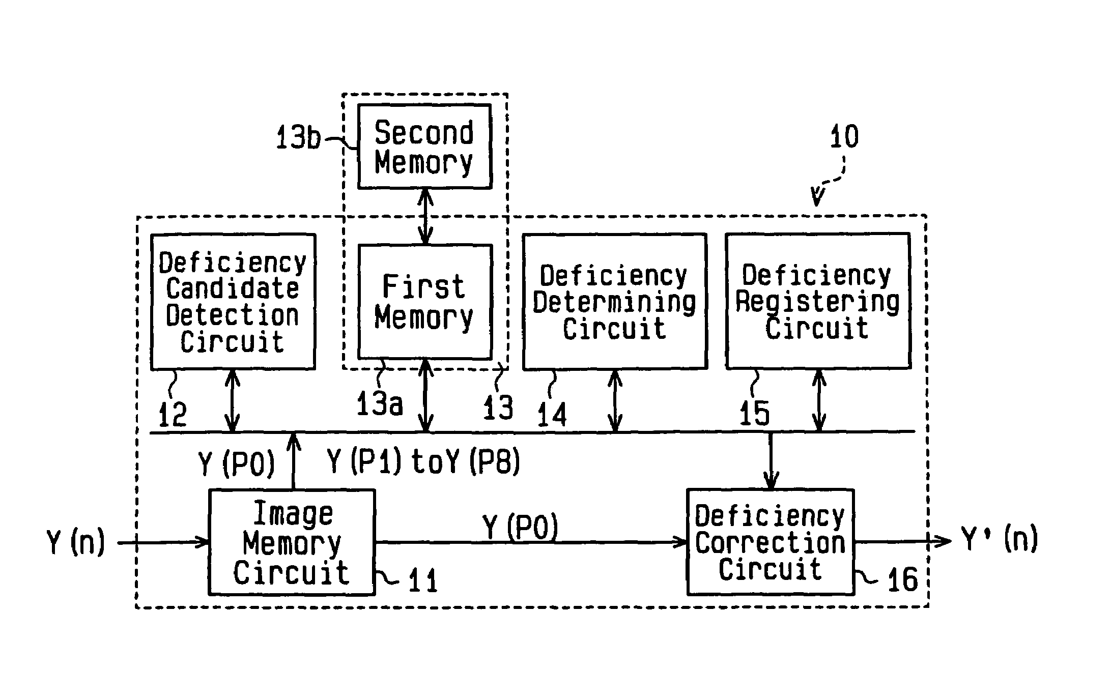
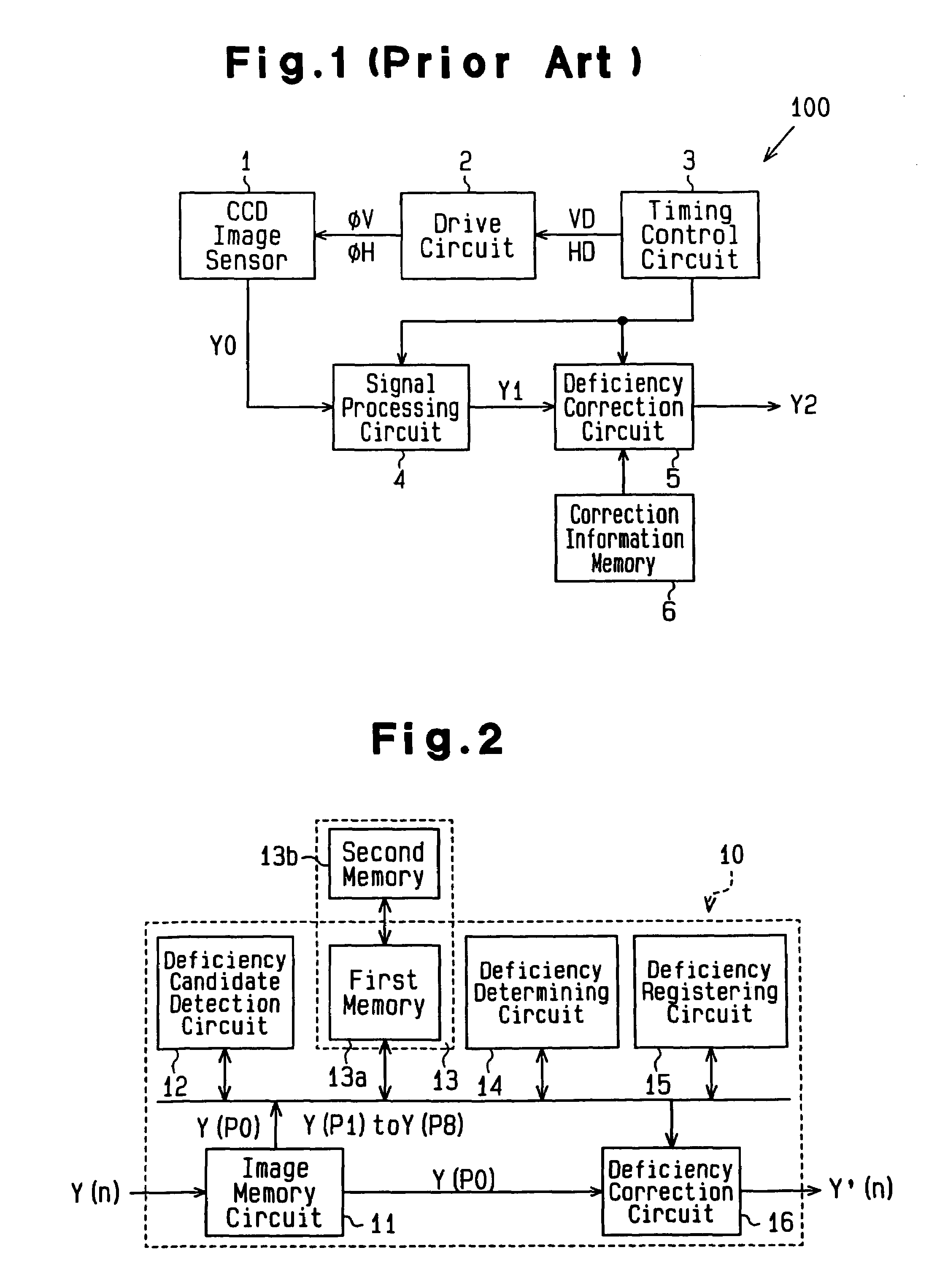
[0034]FIG. 2 is a schematic block diagram of an image signal processor 10 according to the first embodiment of the invention. This image signal processor 10 is adapted for use in a solid state image pickup device.
[0035]As shown in FIG. 2, the image signal processor 10 has an image memory circuit 11, a deficiency candidate detection circuit 12, a position memory circuit 13, a deficiency determining circuit 14, a deficiency registering circuit 15 and a deficiency correction circuit 16. In an image pickup device, a digital image signal Y(n) is produced by performing a predetermined process on the output signal of the image pickup element and then performing A / D conversion on the processed signal. The image signal processor 10 performs correction on the image signal Y(n) of a deficient pixel.
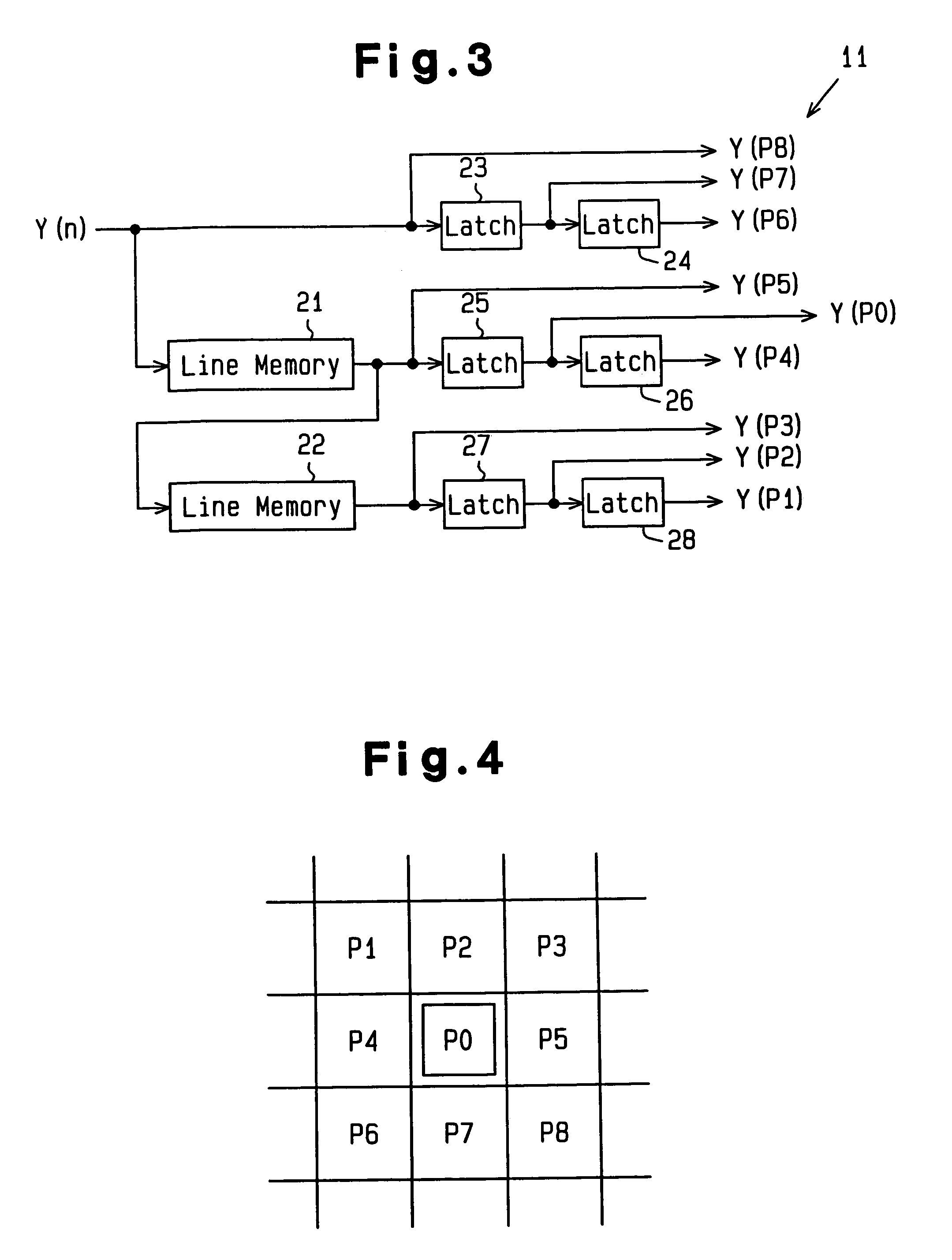
[0036]The image memory circuit 11 has a plurality of line memories 21 and 22 and a plurality of latches 23 to 28 (see FIG. 3). The image memory circuit 11 fetches image signals Y(n) line by line and...
second embodiment
[0086]FIG. 11 is a schematic block diagram of an image signal processor 10A according to the second embodiment of the invention.
[0087]The image signal processor 10A of the second embodiment determines a deficiency of a target pixel using the image pickup conditions of the image pickup device that generates image signals Y(n) in addition to the continuity of a deficient pixel.
[0088]A deficiency determining circuit 14A repeats determination on deficient pixels in accordance with the address information of deficiency candidates stored in the position memory circuit 13, thereby updating the address information. In the determination of a deficiency candidate, for instance with the deficiency candidate detection circuit 12, the deficiency determining circuit 14A determines a deficient pixel, receives information indicating the operational state of the image pickup device and changes the threshold level for determination according to the information.
[0089]When the luminance of the image of...
third embodiment
[0092]FIG. 12 is a schematic block diagram of an image signal processor 10B according to the third embodiment of the invention. The image signal processor 10B of the third embodiment has an area designating circuit 17 in addition to the components of the image signal processor 10 of the first embodiment.
[0093]The image signal processor 10B limits the area of an image where the detection by the deficiency candidate detection circuit 12 is to be carried out. A deficiency determining circuit 14A, like that of the image signal processor 10A of the second embodiment, may determine a deficient pixel by using the image signals Y(n) and image pickup information of the image pickup device.
[0094]The area designating circuit 17 divides one screen into a plurality of sub-areas in synchronism with the horizontal scan timing and vertical scan timing of the image signals Y(n). The area designating circuit 17 controls the deficiency candidate detection circuit 12 in such a way that a deficiency can...
PUM
 Abstract
Description
Claims
Application Information
 - R&D
- Intellectual Property
- Life Sciences
- Materials
- Tech Scout
- Unparalleled Data Quality
- Higher Quality Content
- 60% Fewer Hallucinations
Browse by: Latest US Patents, China's latest patents, Technical Efficacy Thesaurus, Application Domain, Technology Topic, Popular Technical Reports.
© 2025 PatSnap. All rights reserved.Legal|Privacy policy|Modern Slavery Act Transparency Statement|Sitemap|About US| Contact US: help@patsnap.com