Method and apparatus for lowering bus clock frequency in a complex integrated data processing system

Active Publication Date: 2006-08-15
ADVANCED MICRO DEVICES INC
View PDF24 Cites 59 Cited by
  • Summary
  • Abstract
  • Description
  • Claims
  • Application Information

AI Technical Summary

Benefits of technology

[0008]In another form the present invention provides a method for reducing the power consumed by a data processing system. The data processing system has a plurality of devices coupled to a system bus including at least one bus master which is capable of performing accesses on the system bus. At least one of the plurality of devices is clocked using a bus clock sign

Problems solved by technology

However these techniques proved to be inadequate for microprocessors which might, for example, perform periodic functions independent of any user input.
However exit from STOP mode requires a wake-up delay for the clock signals from the oscillator to stabilize before being driven to the microprocessor and STOP mode cannot be used in situations that require fast response to external events.
Many of the I/O peripherals are themselves complex and may be bus

Method used


Image

  • Method and apparatus for lowering bus clock frequency in a complex integrated data processing system
  • Method and apparatus for lowering bus clock frequency in a complex integrated data processing system
  • Method and apparatus for lowering bus clock frequency in a complex integrated data processing system

Examples


Example

DETAILED DESCRIPTION OF THE DRAWINGS

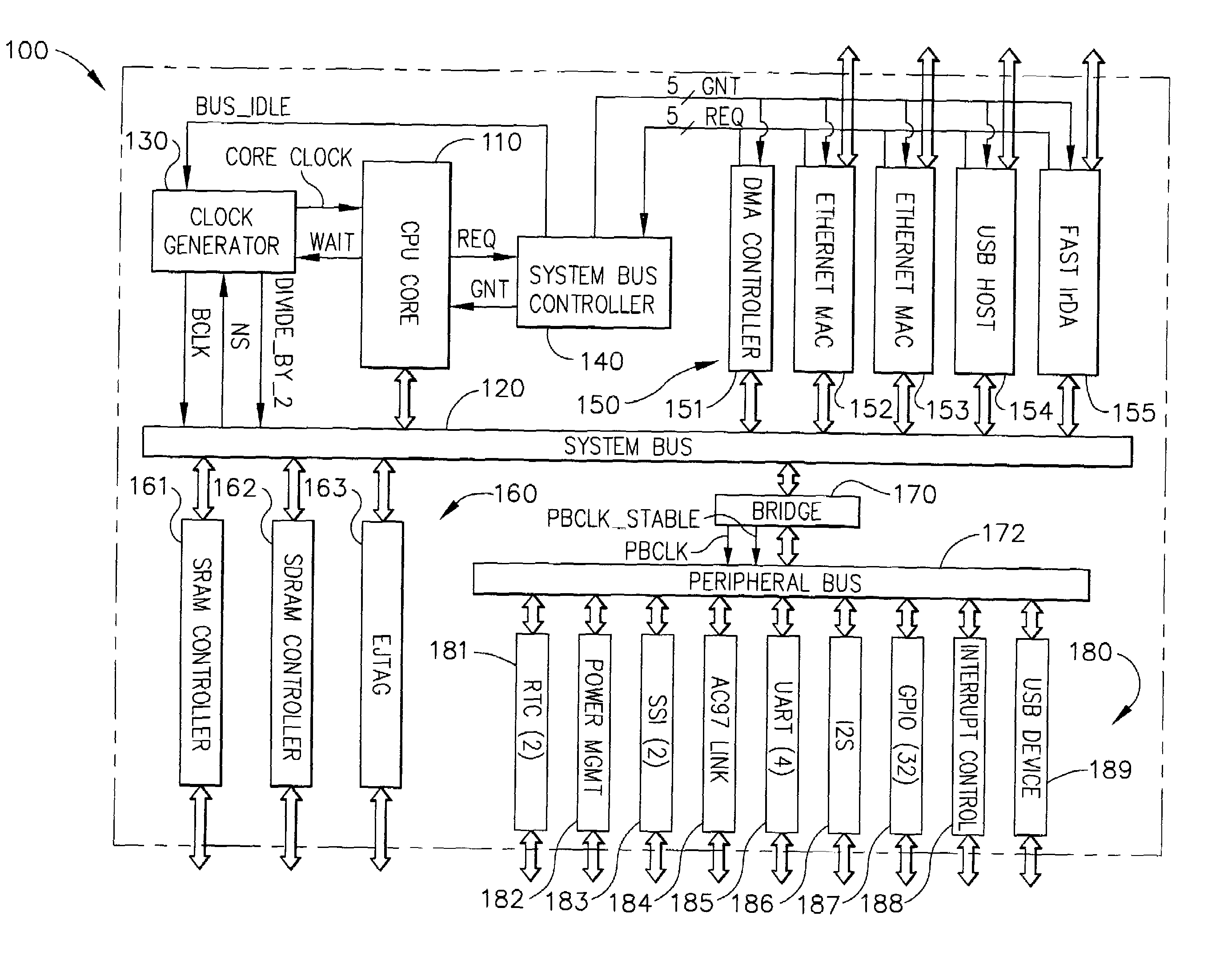
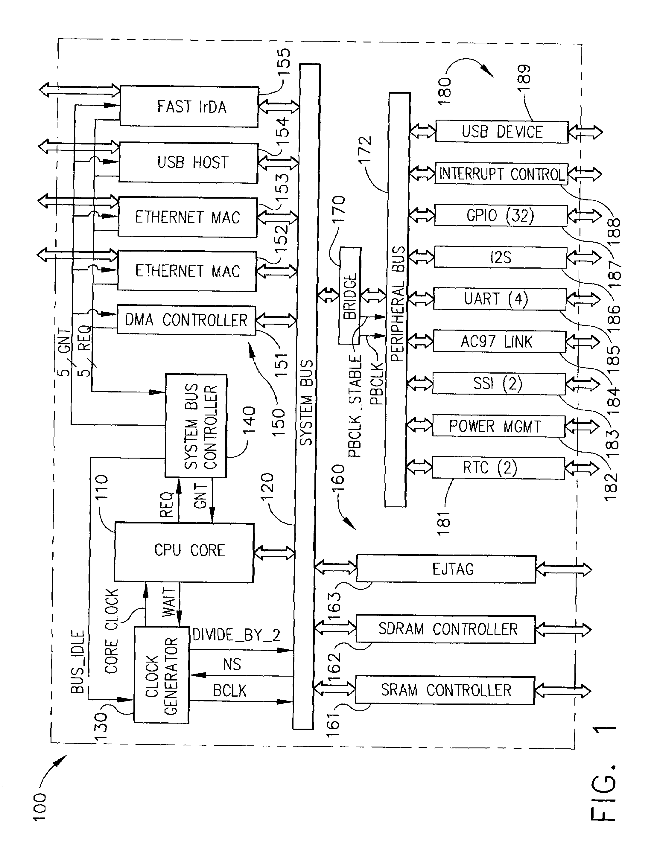
[0016]FIG. 1 illustrates a block diagram of a data processing system 100 according to the present invention. All the devices of data processing system 100 shown in FIG. 1 are combined into a single integrated circuit and thus data processing system 100 is referred to as a system on chip (SOC). Data processing system 100 includes generally a central processing unit (CPU) core 110, a system bus 120, a clock generator 130, a system bus controller 140, a set of bus masters 150, a set of bus slaves 160, a bus bridge 170, a peripheral bus 172, and a set of peripherals 180.

[0017]CPU core 110 is a conventional CPU that is able to fetch instructions and data via system bus 120 and execute the instructions so fetched. In the illustrated embodiment CPU core 110 is a high performance CPU optimized for data intensive applications that executes reduced instruction set computer (RISC) instructions. To support high performance operation for complex SOC tasks it i...


PUM


Abstract

A data processing system (100) comprises a system bus (120), a plurality of devices (110, 150, 160, 170) coupled to the system bus (120), a bus monitor circuit (140), and a clock generator (130). The plurality of devices (110, 150, 160, 170) includes at least one bus master (110, 150) which is capable of performing accesses on the system bus (120). The bus monitor circuit (140) is coupled to the at least one bus master (110, 150), and has an output for providing a bus idle signal to indicate that no bus master is attempting to perform an access on the system bus (120). The clock generator (130) has an output coupled to at least one of the plurality of devices (110, 150, 160, 170) and provides a bus clock signal having a first frequency when the bus idle signal is inactive and having a second frequency lower than the first frequency when the bus idle signal is active.

Description

TECHNICAL FIELD[0001]The present invention relates generally to data processing systems, and more specifically to power reduction for data processing systems.BACKGROUND ART[0002]Low power consumption is an important requirement in the design of data processing systems. For example many applications such as cell phones, personal digital assistants, and the like are powered by a battery. In order to avoid frequent battery changes or the need to connect the battery to a charger, it is desirable that all integrated circuits consume a minimum amount of power. Modern digital integrated circuit fabrication techniques use complementary metal oxide semiconductor (CMOS) transistors which facilitate low power consumption. CMOS logic circuits only consume significant amounts of power when they are switching and integrated circuits built using CMOS technology, or significant portions thereof, may be designed to operate statically, allowing the power to be reduced during periods of inactivity.[00...

Claims


Application Information

Patent Timeline
IPC IPC(8): G06F1/08
CPCG06F1/08G06F1/3203G06F1/3253G06F1/324Y02B60/1235Y02B60/1217Y02D10/00
Inventor WITEK, RICHARD T.PLUMMER, SUZANNEMONTANARO, JAMES JOSEPHKROMER, STEPHEN CHARLESHOOVER, KATHRYN JEAN
Owner ADVANCED MICRO DEVICES INC
Why Eureka
Try Eureka