Semiconductor device and manufacturing method thereof

Active Publication Date: 2006-09-05
SEMICON COMPONENTS IND LLC
View PDF10 Cites 50 Cited by
  • Summary
  • Abstract
  • Description
  • Claims
  • Application Information

AI Technical Summary

Problems solved by technology

Consequently the manufacturing process requires expensive apparatus not used in conventional packaging of semiconductors such as a laser processing machine to process th

Method used


Image

  • Semiconductor device and manufacturing method thereof
  • Semiconductor device and manufacturing method thereof
  • Semiconductor device and manufacturing method thereof

Examples


Embodiment Construction

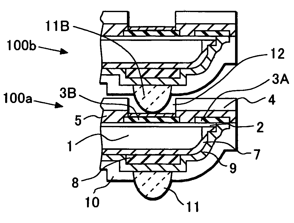
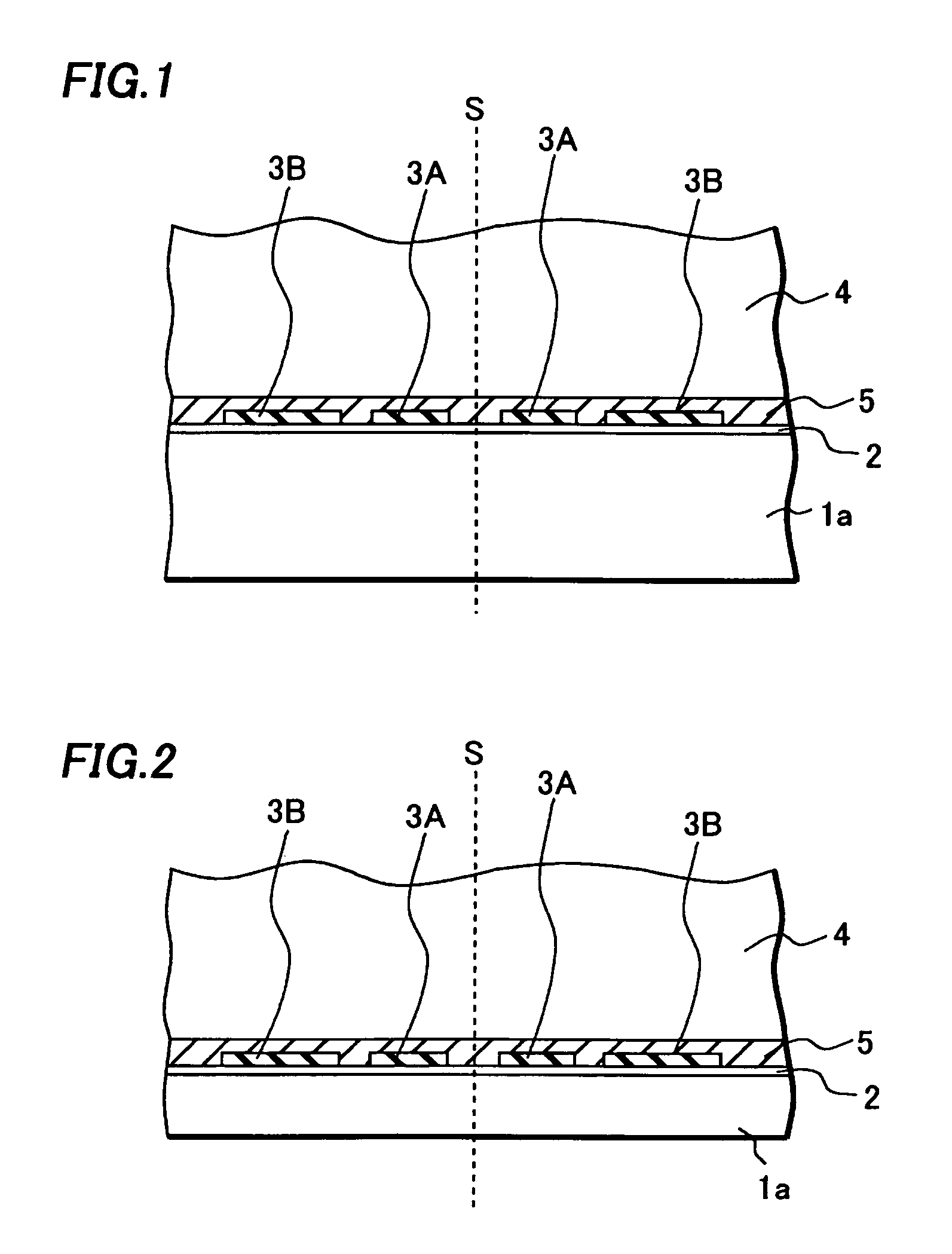
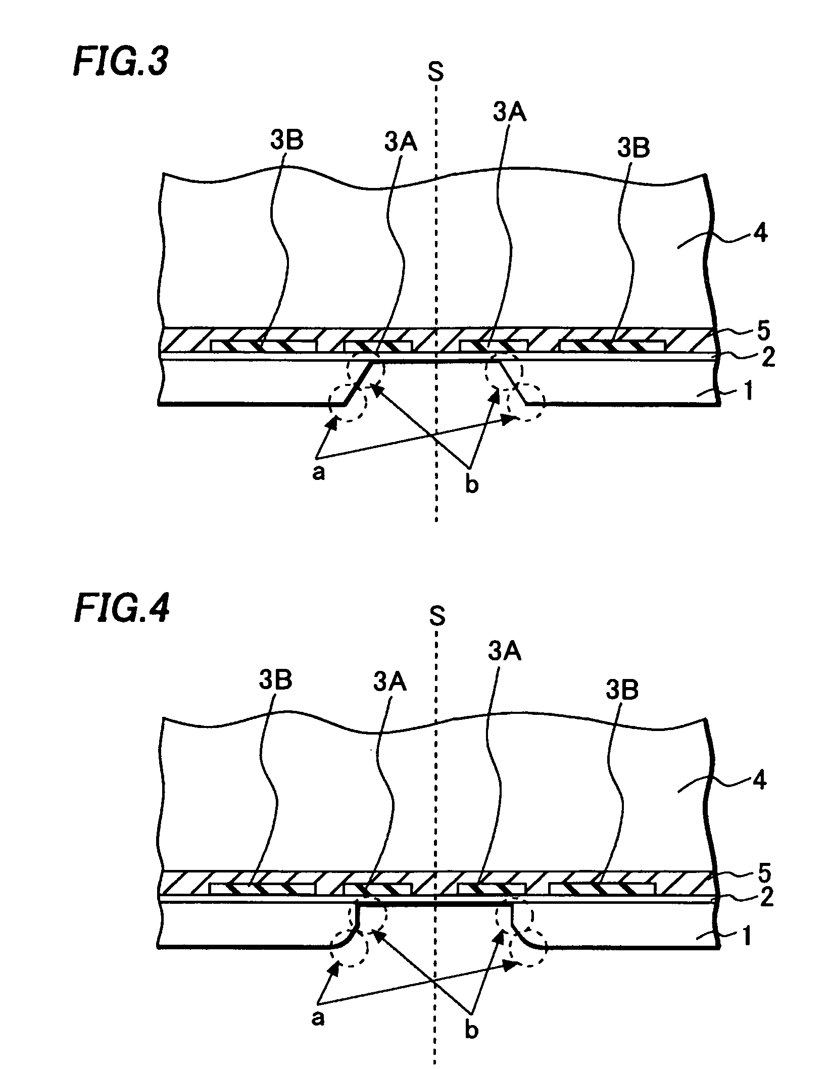
[0025]Next, a semiconductor device and its manufacturing method according to an embodiment of this invention will be described, referring to FIGS. 1 through 13.

[0026]First, a semiconductor wafer 1a is provided, as shown in FIG. 1. The semiconductor wafer 1a will be cut into a plurality of semiconductor chips 1 in a process step which will be described later. The semiconductor chips 1 are CCD (Charge Coupled Device) image sensors or semiconductor memory chips, for example, and are manufactured by semiconductor wafer processing. A plurality of first wirings 3A and a plurality of second wirings 3B are formed on a surface of the semiconductor wafer 1a through an insulation film 2 simultaneously. The first wirings 3A are formed to have a predetermined length of separation from each other across a border S along which the semiconductor wafer 1a is to be cut into the plurality of semiconductor chips 1. The border S is called a dicing line or a scribe line.

[0027]The first wiring 3A is to pl...


PUM


Abstract

A stacked MCM is manufactured at reduced cost without using expensive apparatus. A first wiring and a second wiring are formed on a surface of a semiconductor chip of a first semiconductor device through an insulation film. A glass substrate having an opening to expose the second wiring is bonded to the surface of the semiconductor chip on which the first wiring and the second wiring are formed. A third wiring is disposed on a back surface and a side surface of the semiconductor chip through an insulation film and connected to the first wiring. And a conductive terminal of another semiconductor device is connected to the second wiring through the opening.

Description

CROSS-REFERENCE OF THE INVENTION[0001]This invention is based on Japanese Patent Application No. 2003-120228, the content of which is incorporated by reference in its entirety.BACKGROUND OF THE INVENTION[0002]1. Field of the Invention[0003]This invention relates to a semiconductor device and its manufacturing method specifically to a packaging technology of a semiconductor chip.[0004]2. Description of the Related Art[0005]An MCM (Multi-Chip Module) has received attention in recent years as a new packaging technology. The MCM is a high performance module implemented by incorporating a plurality of semiconductor chips into a single package. There are various kinds of MCMs depending on how the semiconductor chips are placed. Among them, attention is focused on a “stacked MCM” which is made by stacking a plurality of semiconductor chips.[0006]An example of the stacked MCM structure is shown in FIG. 14. The stacked MCM 200 is made by stacking a plurality of semiconductor chips 204. Via h...

Claims


Application Information

Patent Timeline
IPC IPC(8): H01L23/48H01L23/52H01L29/40H01L23/50H01L21/768H01L23/31H01L23/485H01L25/065H01L27/148
CPCH01L21/76898H01L24/02H01L25/0657H01L27/14806H01L23/3114H01L2225/06565H01L2224/0401H01L2224/16H01L2924/01005H01L2924/01014H01L2924/01028H01L2924/01029H01L2924/01033H01L2924/01078H01L2924/01079H01L2924/014H01L2924/01047H01L2225/06527H01L2225/06517H01L2225/06513H01L2924/12042H01L2224/06181H01L2224/06182H01L2224/16147H01L2924/0001H01L24/03H01L24/05H01L24/06H01L24/13H01L24/16H01L2224/05548H01L2224/13024H01L2224/02371H01L2224/02125H01L2224/13022H01L2924/00H01L2224/02E06B7/215E06B7/36E06B3/02E05Y2800/41
Inventor NOMA, TAKASHISUZUKISHINOGI, HIROYUKI
Owner SEMICON COMPONENTS IND LLC
Why Eureka
Try Eureka