Pulsed quantum dot laser system with low jitter

a quantum dot laser and laser system technology, applied in the field of quantum dot lasers, can solve the problems of low jitter, and achieve the effects of low phase noise, low jitter, and low jitter

Inactive Publication Date: 2006-09-05
APPLIED MATERIALS INC
View PDF79 Cites 23 Cited by
  • Summary
  • Abstract
  • Description
  • Claims
  • Application Information

AI Technical Summary

Benefits of technology

[0008]In general, in one aspect, the invention features a pulsed laser or laser system with low phase noise resulting in low jitter. The laser includes a region of quantum dots (e.g. the gain section) made of, for example, InAs or InGaAs grown on GaAs, AlGaAs or InGaAs. The quantum dots within that region are grown so as to produce a continuous distribution of sizes, shapes, compositions, and / or environments randomly arranged throughout the region. This random and relatively broad distribution of quantum dots achieves automatic matching with cavity resonance. That, in combination with also taking additional measures and / or optionally including additional sections within the laser for phase or wavelength control and amplification results in very low jitter. This particular category of quantum dot (QD) laser diodes has the advantage of being capable of generating reduced or low jitter without the need for a phase noise reduction loop. Thus, in this case, the laser or laser system lends itself to being specifically applied to generating an optical clock or sampling signal for which low jitter is an important requirement.
[0009]The pulsed laser diodes that include quantum dots having a broad distribution of sizes enable one to generate optical clock signals with high precision, i.e., characterized by short pulses, high repetition (clock) rates, and low jitter (variation in inter-pulse time interval and amplitude).
[0010]Some of the QD laser diodes of the type described herein are grown on a GaAs (gallium arsenide) substrate to operate at wavelengths in the transparency range of bulk silicon (i.e., longer than 1100 nm). In comparison, conventional (e.g. bulk and quantum well) laser diodes that are designed to emit in that wavelength range require InGaAsP (indium gallium arsenide phosphide) or other quaternary alloys lattice-matched to InP (indium phosphide) substrates. Because GaAs based growth and fabrication processes are much more developed, have higher production yields, and are lower cost than the InP based growth and fabrication processes, this represents a significant advantage.
[0011]In addition, compared to InP based lasers, QD laser diodes of the type described herein offer lower dependence on ambient temperature and thereby permit simplification or elimination of the customary temperature controls used in laser diode systems. They may be made less sensitive to optical feedback reflections and thereby permit simplification or elimination of the customary optical isolation used in laser diode systems. What is especially novel is the application of single or coupled quantum dot lasers to optical clocking or data sampling, given the importance of reduced temperature sensitivity, reduced feedback instabilities, low jitter, silicon transparency wavelength range, and low cost high volume production based on gallium arsenide technology.

Problems solved by technology

That, in combination with also taking additional measures and / or optionally including additional sections within the laser for phase or wavelength control and amplification results in very low jitter.

Method used


Image

  • Pulsed quantum dot laser system with low jitter
  • Pulsed quantum dot laser system with low jitter
  • Pulsed quantum dot laser system with low jitter

Examples


Embodiment Construction

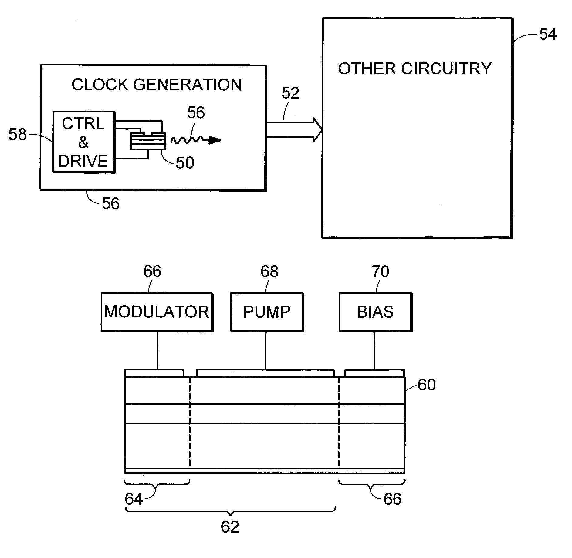
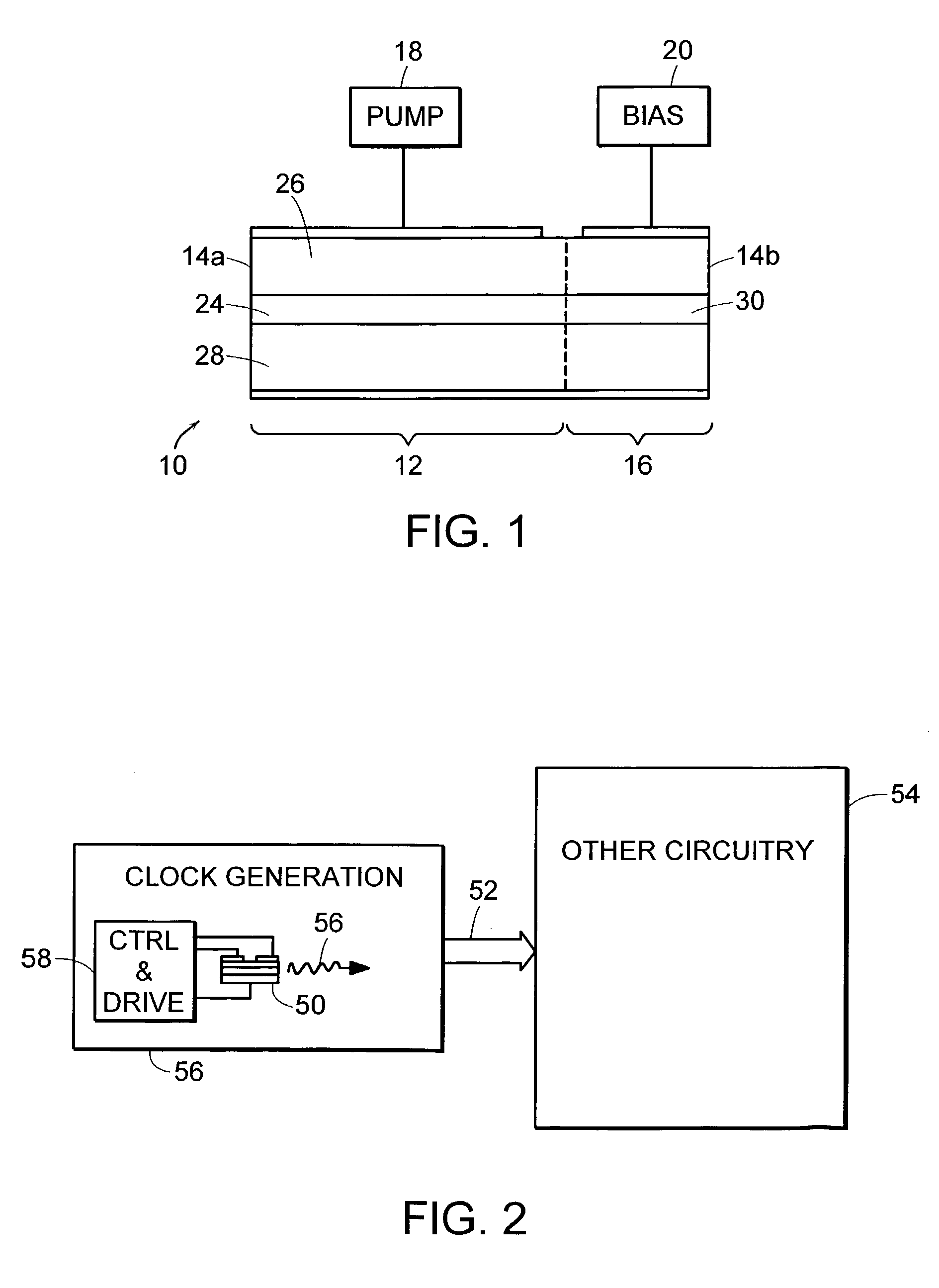
[0024]Referring to FIG. 1, one exemplary embodiment is a laser diode 10 which incorporates into its structure at least one region having a broad random statistical distribution of quantum dots of different sizes, shapes, compositions, and / or environments. As will be discussed in greater detail below, this broad distribution of quantum dots produces in the laser diode structure a correspondingly broad distribution of emission wavelengths which, in turn, greatly facilitates matching to cavity modes within the laser diode.

[0025]Laser diode 10 includes an optically amplifying medium forming a gain element or gain section 12 within a cavity formed by two partially reflecting surfaces or mirrors 14a and 14b located on opposite sides of the device. Mirrors 14a and 14b can be formed by cleaving the ends of the device to form surfaces which contact the air and produce a reflectivity of about 30%. Mirrors 14a and 14b provide optical feedback according to which a portion of the amplified light...


PUM


Abstract

A circuit for generating a clock or sampling signal, the circuit including: a semiconductor quantum dot laser element including a region of quantum dots, wherein the region of quantum dots is characterized by an emission distribution having a half-width of at least about 10 meV; and drive circuitry connected to the quantum dot laser element for operating the quantum dot laser element as a mode-locked laser that outputs a periodic, uniformly spaced sequence of pulses, wherein the clock or sampling signal is derived from the sequence of pulses.

Description

[0001]This application claims the benefit of U.S. Provisional Application No. 60 / 483,354, filed Jun. 27, 2003.TECHNICAL FIELD[0002]This invention relates to quantum dot lasers and their applications.BACKGROUND OF THE INVENTION[0003]Quantum dots are three-dimensional semiconductor structures that confine electrons and holes in 3-dimensions and thereby produce energy quantization. Quantum dots are so small that quantum mechanical effects come into play in controlling their behavior. The “dots,” which up close actually appear to be more pyramidal in shape, have base dimensions on the order of about 200 Å and height dimensions of about 80 Å.[0004]Some years ago, the scientific community realized that one could make a new type of semiconductor laser by using quantum dots in the active layer. Those new lasers, referred to as quantum dot lasers, held out the promise of great benefits. For example, it was expected that the quantum dot lasers would exhibit less-temperature dependent performa...

Claims


Application Information

Patent Timeline
Patent Type & Authority Patents(United States)
IPC IPC(8): H01S3/00H01SH01S3/098H01S5/00H01S5/026H01S5/06H01S5/065H01S5/34H01S5/40H04B10/00H04L7/00
CPCB82Y10/00B82Y20/00H01S5/0265H04L7/0075H04B10/00H01S5/065H01S5/0064H01S5/026H01S5/0602H01S5/0657H01S5/3412H01S5/4006H01S2301/04H01S5/30H01S3/00H01S5/10
Inventor MCINERNEY, JOHN G.WOJCIK, GREGORY L.WEST, LAWRENCE C.
Owner APPLIED MATERIALS INC
Why Eureka
Try Eureka