Method of making chip resistor

a chip and resistor technology, applied in resistive material coating, instruments, record information storage, etc., can solve the problems of reducing production efficiency, preventing the mounting of excess, and reducing the yielding percentage, so as to prevent the mounting from rejecting

Inactive Publication Date: 2006-09-12
ROHM CO LTD
View PDF8 Cites 10 Cited by
  • Summary
  • Abstract
  • Description
  • Claims
  • Application Information

AI Technical Summary

Benefits of technology

[0013]It is therefore an object of the present invention to provide a method of making a chip resistor to provide the chip resistor containing no leads, to properly adjust a resistance of a resistor material, and further to prevent a rejection in mounting caused by a miniaturization of the chip and a reduction of a yielding percentage.

Problems solved by technology

However, considering environmental problems, it is undesirable to use a lead-contained glass paste.
However, the miniaturization of the chip leads to a width reduction of the dividing grooves 97A, 97B, which impedes the removal of the excess remaining in the dividing grooves 97A, 97B.
Further, the additional process of etching results in a decline in production efficiency.
A second problem is an increase in rejection rates in mounting.
In particular, the small chip is greatly influenced in shape by being chipped off, which tends to lead to the increase in rejection rates in mounting.
A third problem is a decrease in yielding percentage.
As a result, the increase in rejection rate leads to the decrease in yielding percentage, which increases manufacturing costs.

Method used


Image

  • Method of making chip resistor
  • Method of making chip resistor
  • Method of making chip resistor

Examples


Embodiment Construction

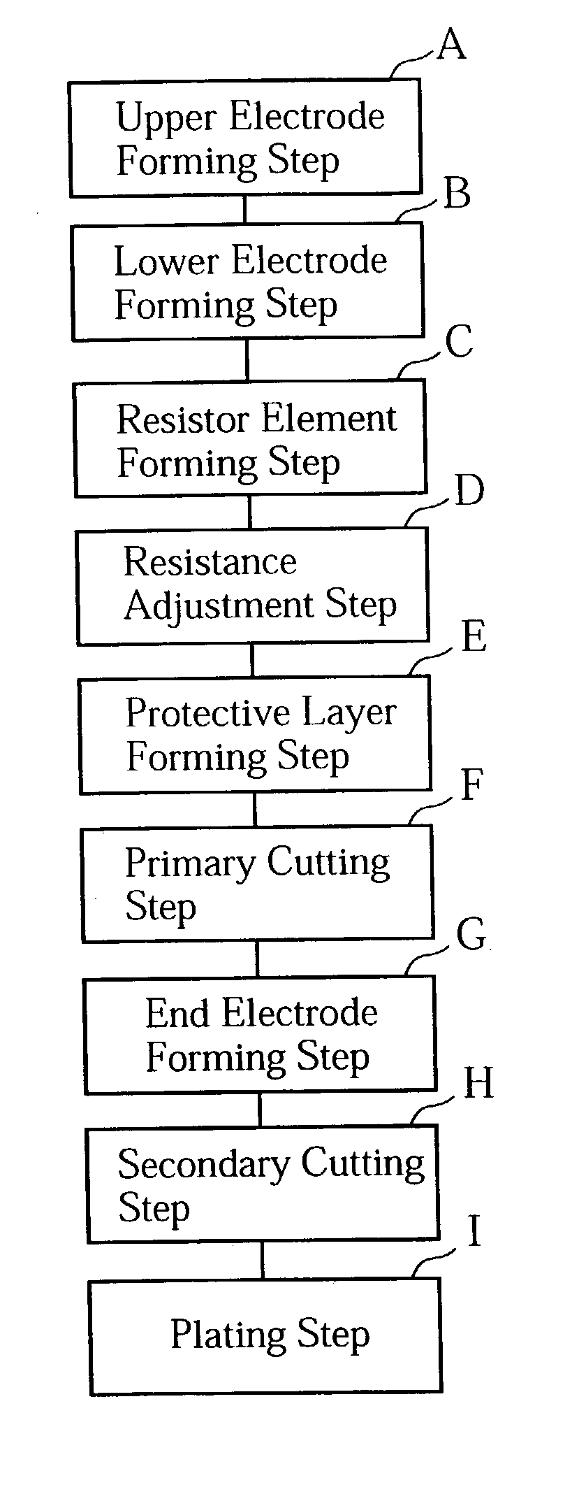
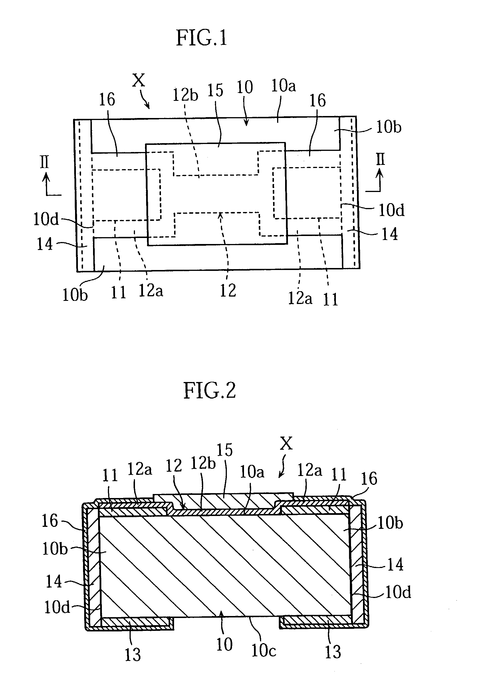
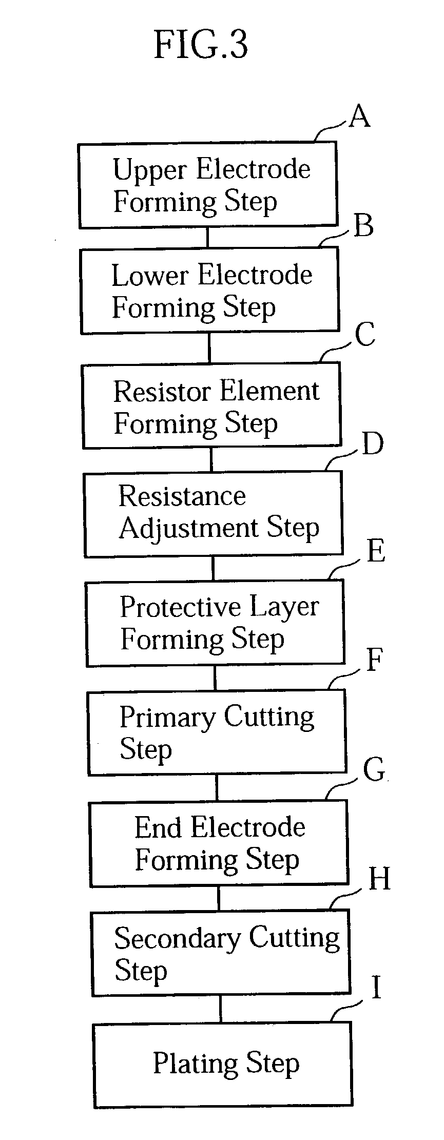
[0057]A chip resistor X illustrated in FIGS. 1 and 2 comprises an insulating substrate 10, a pair of upper electrodes 11, a resistor element 12, a pair of lower electrodes 13, a pair of end electrodes 14, a protective layer 15 and plating layers 16.

[0058]The insulating substrate 10 is in the form of a substantially rectangular parallelepiped, made of insulating material such as alumina.

[0059]The pair of upper electrodes 11 are spaced apart from each other on an upper surface 10a of the insulating substrate 10. Each upper electrode 11 is formed by printing and baking a metal organic paste in a thick layer having a thickness of 2000–3000 Å for example.

[0060]The resistor element 12 is formed on the upper surface 10a of the insulating substrate 10 so as to connect between the paired upper electrodes 11. The resistor element 12, made of Ni—Cr or Ta, is in the form of a thin film having a thickness of 1000–2000 Å for example. The resistor element 12 includes an end portion 12a entirely co...


PUM

PropertyMeasurementUnit
thicknessaaaaaaaaaa
thicknessaaaaaaaaaa
thickaaaaaaaaaa

Abstract

The invention relates to a method of making a chip resistor using a material substrate for which are set a plurality of first cutting lines extending in a first direction and a plurality of second cutting lines extending in a second direction perpendicular to the first direction. The method includes an upper electrode forming step A for forming a thick upper conductor layer on the upper surface of the substrate by printing and baking a metal organic paste, a lower electrode forming step B for forming a thick lower conductor layer on the lower surface of the substrate by printing and baking metal organic paste, and a resistor element forming step C for forming a thin resistor layer by depositing a resistor material on the upper surface of the substrate. Preferably, the upper and the lower surfaces of the material substrate are flat.

Description

BACKGROUND OF THE INVENTION[0001]1. Field of the Invention[0002]The present invention relates to a chip resistor provided with a thin-film resistor element, and also to a method of making the same.[0003]2. Description of the Related Art[0004]FIGS. 14 and 15 illustrate a chip resistor. The chip resistor 9 shown in these figures includes a insulating substrate 90, a pair of upper electrodes 91, a resistor element 92 connecting the paired upper electrodes 91, a pair of lower electrodes 93, a pair of end electrodes 94 connecting the upper electrodes 91 and the lower electrodes 93, a protective layer 95 covering the resistor element 92, and plating layers 96 for covering the electrodes 91, 93, 94.[0005]The chip resistor 9, as shown in FIG. 16A, may be manufactured from a material substrate 9A which is formed with a plurality of dividing grooves 97A, 97B extending vertically and horizontally and setting a plurality of chip resistor forming regions 98 arranged vertically and horizontally.[...

Claims


Application Information

Patent Timeline
Patent Type & Authority Patents(United States)
IPC IPC(8): H01C17/00H01C1/012H01C17/06H01C7/00H01C17/28
CPCH01C7/003H01C17/006H01C17/281Y10T29/49101Y10T29/49128Y10T29/49135Y10T29/4913Y10T29/49052Y10T29/49082Y10T29/49099
Inventor TANIMURA, MASANORI
Owner ROHM CO LTD
Why Eureka
Try Eureka